
LP2980LV
Micropower SOT, 50 mA Low-Voltage Low-Dropout
Regulator For Applications With Output Voltages
<
2V
General Description
The LP2980LV is a 50 mA, fixed-output voltage regulator
designed for high performance in applications requiring out-
put voltages below 2V.
Using an optimized VIP
TM
(Vertically Integrated PNP) pro-
cess, the LP2980LV delivers unequalled performance in all
specifications critical to battery-powered designs:
Low Ground Pin Current. Typically 280 µA
@
50 mA load,
and 75 µA
@
1 mA load.
Sleep Mode. Less than 1 µA quiescent current when ON/
OFF pin is pulled low.
Smallest Possible Size. SOT-23 package uses absolute
minimum board space.
Precision Output. 0.5% tolerance output voltages available
(A grade).
Features
n
Guaranteed 50 mA output current
n
Smallest possible size (SOT-23 Package)
n
Requires few external components
n
<
1 µA quiescent current when shutdown
n
Low ground pin current at all load currents
n
Output voltage accuracy 0.5% (A Grade)
n
High peak current capability (150 mA typical)
n
Wide supply voltage range (16V max)
n
Fast dynamic response to line and load
n
Low Z
OUT
0.1
typical (10 Hz to 1 MHz)
n
Overtemperature/overcurrent protection
n
-40∞C to +125∞C junction temperature range
Applications
n
Cellular Phone
n
Palmtop/Laptop Computer
n
Personal Digital Assistant (PDA)
n
Camcorder, Personal Stereo, Camera
Block Diagram
10109101
VIP
TM
is a trademark of National Semiconductor Corporation.
May 2002
LP2980L
V
Micropower
SOT
,
5
0
m
A
Low-V
oltage
Low-Dropout
Regulator
For
Applications
W
ith
Output
V
oltages
<
2V
© 2002 National Semiconductor Corporation
DS101091
www.national.com
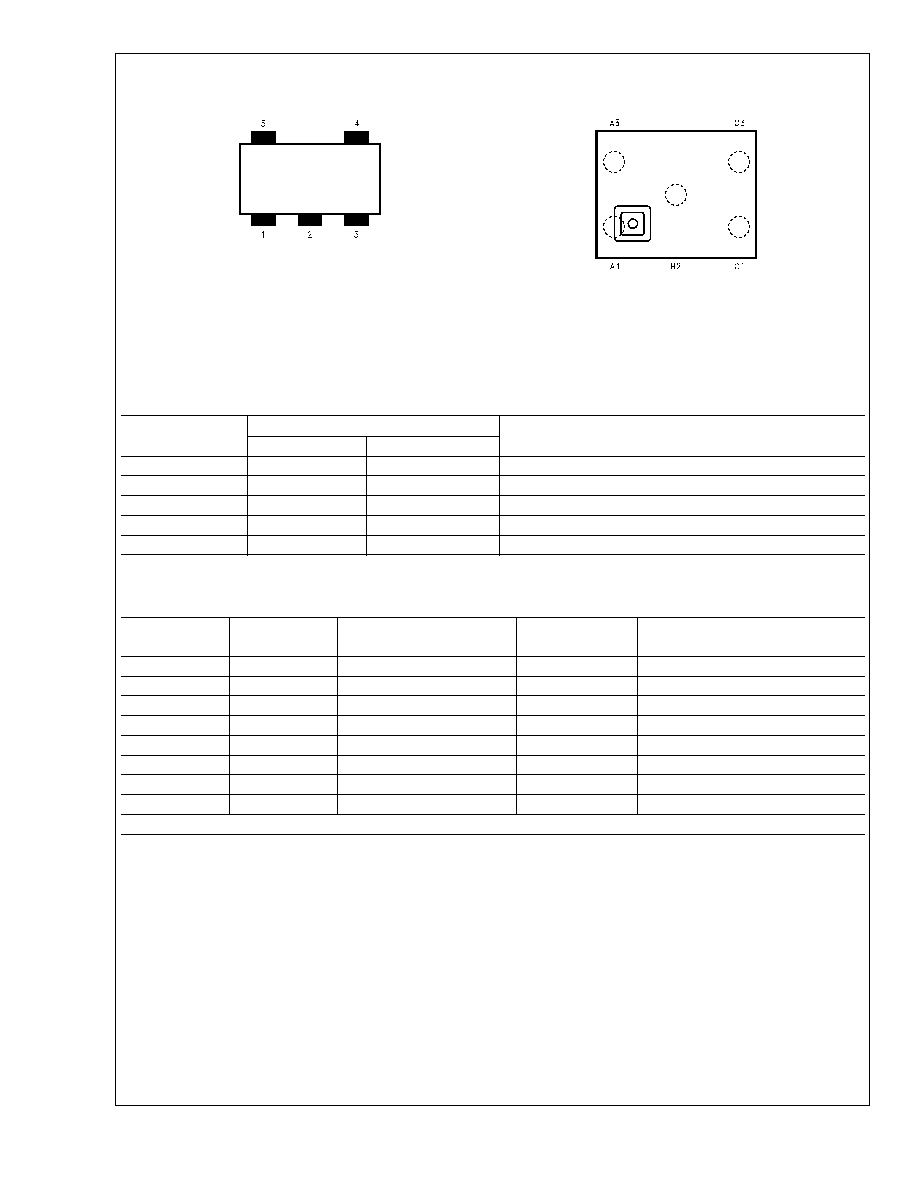
Connection Diagrams
5-Lead Small Outline Package (M5)
micro SMD, 5 Bump Package (BPA05)
10109102
Top View
See NS Package Number MF05A
For ordering information see
Table 1
10109157
Top View
See NS Package Number BPA05
Note: The actual physical placement of the package marking will vary from
part to part. The package marking will designate the date code and will vary
considerably. Package marking does not correlate to device type in any way.
Pin Descrption
Name
Pin Number
Function
SOT-23
micro SMD
V
IN
1
C3
Input Voltage
GND
2
A1
Common Ground (device substrate)
ON/OFF
3
A3
Logic high enable input
N/C
4
B2
Post package trim - do not connect to this pin
V
OUT
5
C1
Regulated output voltage
Ordering Information
TABLE 1. Package Marking and Ordering Information
Output Voltage
(V)
Grade
Order Information
Package Marking
Supplied as:
1.5V
A
LP2980AIM5X-1.5
LANA
3000 Units on Tape and Reel
1.5V
A
LP2980AIM5-1.5
LANA
1000 Units on Tape and Reel
1.5V
STD
LP2980IM5X-1.5
LANB
3000 Units on Tape and Reel
1.5V
STD
LP2980IM5-1.5
LANB
1000 Units on Tape and Reel
1.8V
A
LP2980AIM5X-1.8
LAGA
3000 Units on Tape and Reel
1.8V
A
LP2980AIM5-1.8
LAGA
1000 Units on Tape and Reel
1.8V
STD
LP2980IM5X-1.8
LAGB
3000 Units on Tape and Reel
1.8V
STD
LP2980IM5-1.8
LAGB
1000 Units on Tape and Reel
For output voltages
>
2V, refer to LP2980 datasheet. If a non-standard voltage is required, see LP2980-ADJ.
LP2980L
V
www.national.com
2
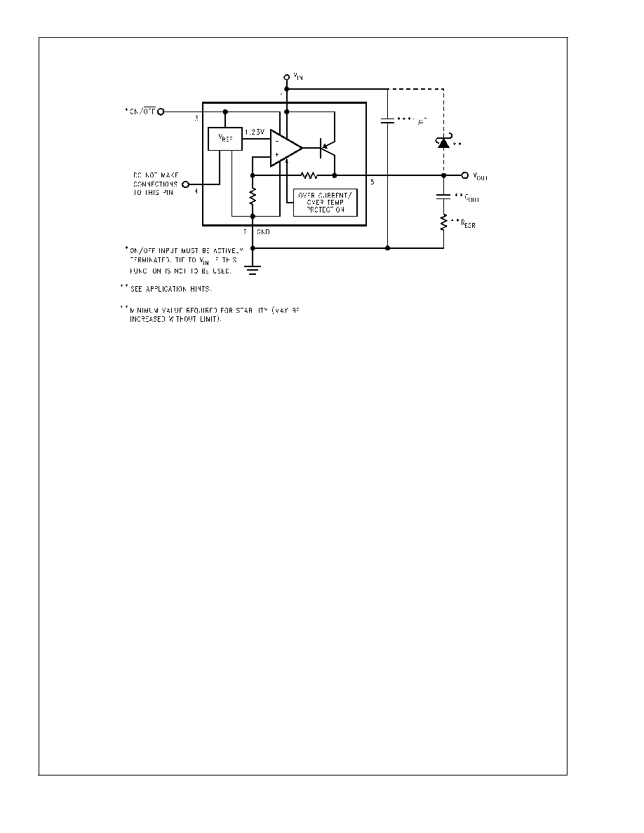
Basic Application Circuit
10109103
LP2980L
V
www.national.com
3
Absolute Maximum Ratings
(Note 1)
If Military/Aerospace specified devices are required,
please contact the National Semiconductor Sales Office/
Distributors for availability and specifications.
Storage Temperature Range
-65∞C to +150∞C
Operating Junction Temperature
Range
-40∞C to +125∞C
Lead Temperature
(Soldering, 5 sec.)
260∞C
ESD Rating (Note 2)
2 kV
Power Dissipation (Note 3)
Internally Limited
Input Supply Voltage (Survival)
-0.3V to +16V
Input Supply Voltage (Operating)
2.1V to +16V
ON/OFF Input Voltage (Survival)
-0.3V to +16V
Output Voltage (Survival), (Note
4)
-0.3V to +9V
I
OUT
(Survival)
Short Circuit Protected
Input-Output Voltage (Survival),
(Note 5)
-0.3V to +16V
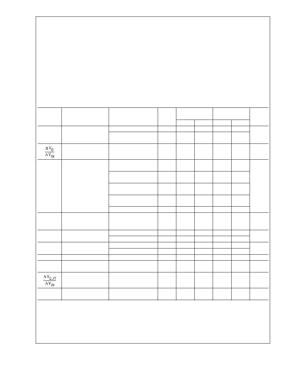
Electrical Characteristics
Limits in standard typeface are for T
J
= 25∞C, and limits in boldface type apply over the full operating temperature range. Un-
less otherwise specified: V
IN
= V
O(NOM)
+ 1V, I
L
= 1 mA, C
IN
= 1 µF, C
OUT
= 4.7 µF, V
ON/OFF
= 2V.
Symbol
Parameter
Conditions
Typ
LP2980LVAI-XX
(Note 6)
LP2980LVI-XX
(Note 6)
Units
Min
Max
Min
Max
V
O
Output Voltage
Tolerance
I
L
= 1 mA
-0.50
0.50
-1.00
1.00
%V
NOM
1 mA
<
I
L
<
50 mA
-0.75
-2.50
0.75
2.50
-1.50
-3.50
1.50
-3.50
Output Voltage Line
Regulation
V
O(NOM)
+ 1V
V
IN
16V
0.007
0.014
0.032
0.014
0.032
%/V
I
GND
Ground Pin Current
I
L
= 0
65
85
110
85
110
µA
I
L
= 1 mA
75
95
160
95
160
I
L
= 10 mA
120
175
325
175
325
I
L
= 50 mA
280
475
850
475
850
V
ON/OFF
<
0.18V
0
1
1
V
IN
(min)
Minimum input voltage
required to maintain
output regulation
I
L
= 50 mA
2.05
2.20
2.20
V
V
ON/OFF
ON/OFF Input Voltage
(Note 7)
High = O/P ON
1.4
1.6
1.6
V
Low = O/P OFF
0.55
0.18
0.18
I
ON/OFF
ON/OFF Input Current
V
ON/OFF
= 0
0
-1
-1
µA
V
ON/OFF
= 5V
5
15
15
I
O(PK)
Peak Output Current
V
OUT
V
O(NOM)
- 5%
150
100
100
mA
e
n
Output Noise Voltage
(RMS)
BW = 300 Hz to 50 kHz,
C
OUT
= 10 µF
125
µV
Ripple Rejection
f = 1kHz C
OUT
= 10 µF
63
dB
I
O(MAX)
Short Circuit Current
R
L
= 0 (Steady State)
(Note 8)
150
mA
Note 1: Absolute maximum ratings indicate limits beyond which damage to the component may occur. Electrical specifications do not apply when operating the
device outside of its rated operating conditions.
Note 2: The ESD rating of pins 3 and 4 is 1 kV.
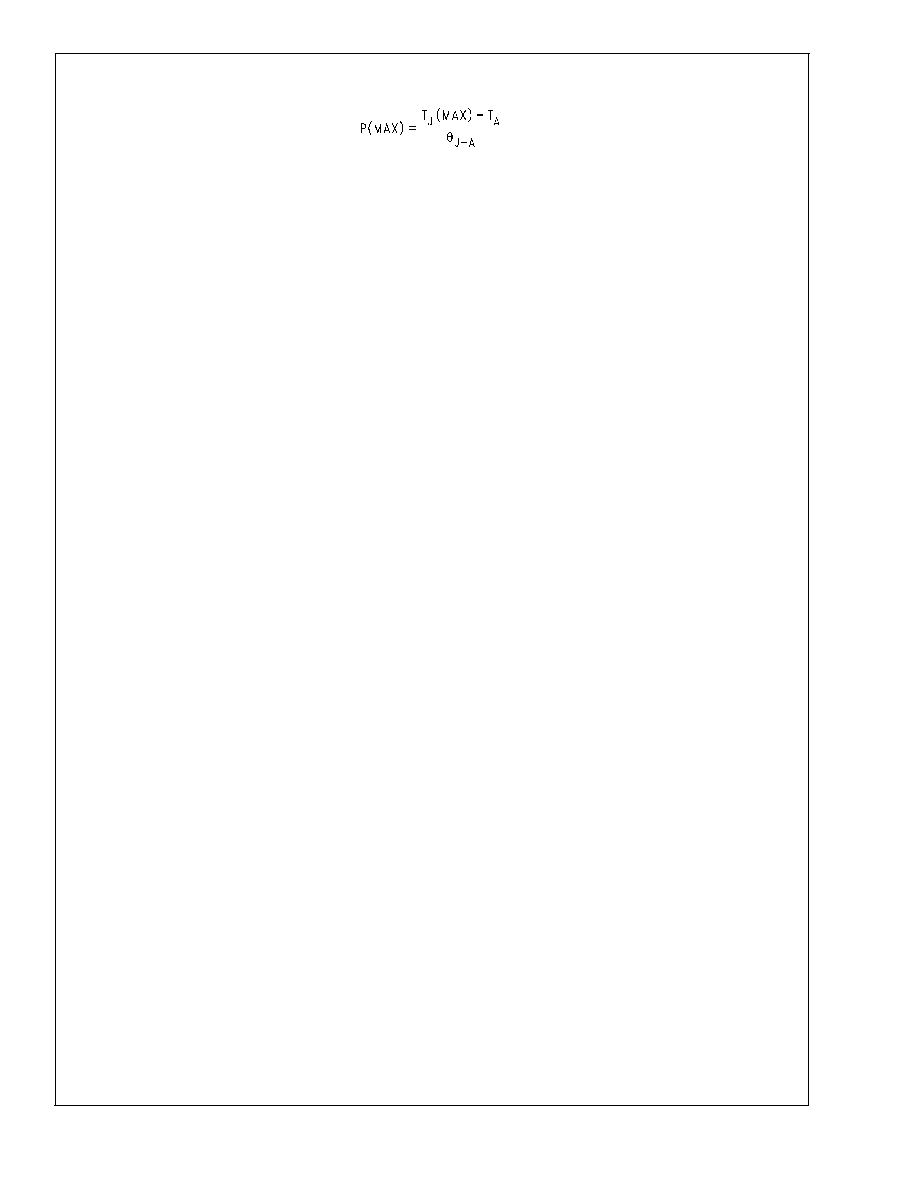
Note 3: The maximum allowable power dissipation is a function of the maximum junction temperature, T
J(MAX)
, the junction-to-ambient thermal resistance,
JA
, and
the ambient temperature, T
A
. The maximum allowable power dissipation at any ambient temperature is calculated using:
LP2980L
V
www.national.com
4
Electrical Characteristics
(Continued)
The value of
JA
for the SOT-23 package is 220∞C/W. Exceeding the maximum allowable power dissipation will cause excessive die temperature, and the regulator
will go into thermal shutdown.
Note 4: If used in a dual-supply system where the regulator load is returned to a negative supply, the LP2980LV output must be diode-clamped to ground.
Note 5: The output PNP structure contains a diode between the V
IN
and V
OUT
terminals that is normally reverse-biased. Reversing the polarity from V
IN
to V
OUT
will turn on this diode and possibly damage the device (see Application Hints).
Note 6: Limits are 100% production tested at 25∞C. Limits over the operating temperature range are guaranteed through correlation using Statistical Quality Control
(SQC) methods. The limits are used to calculate National's Average Outgoing Quality Level (AOQL).
Note 7: The ON/OFF input must be properly driven to prevent misoperation. For details, refer to Application Hints.
Note 8: See Typical Performance Characteristics curves.
LP2980L
V
www.national.com
5
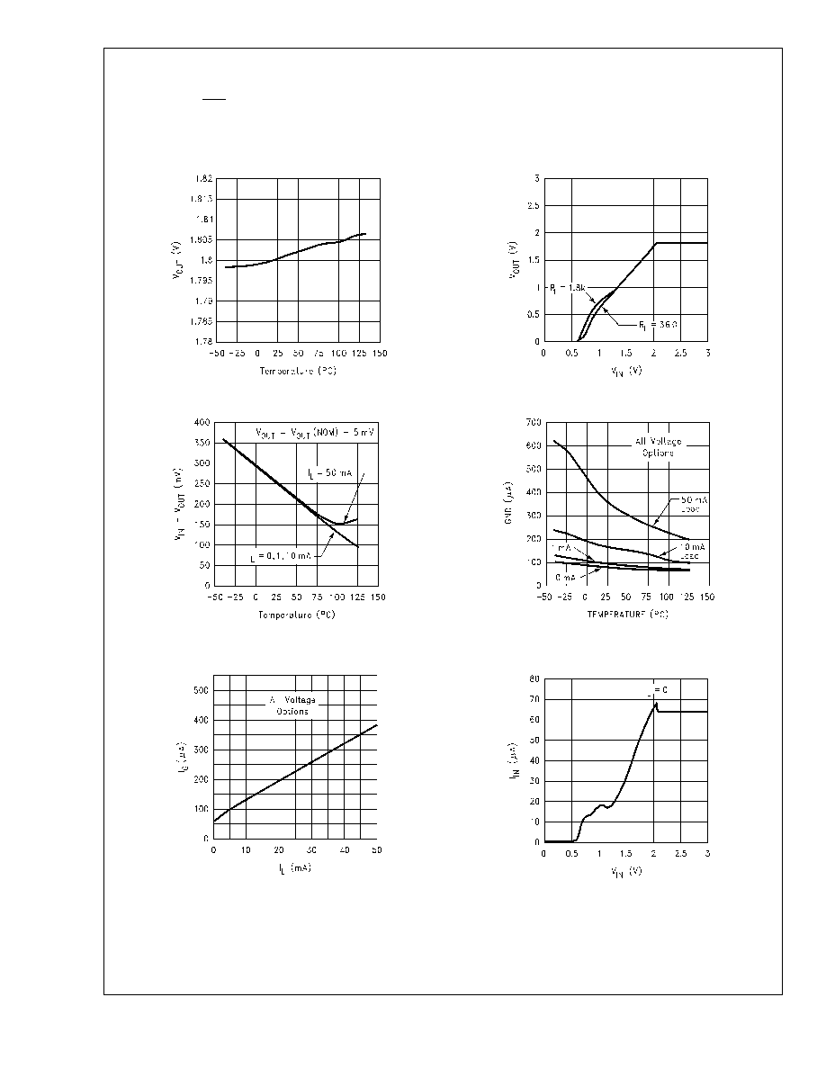
Typical Performance Characteristics
Unless otherwise specified: T
A
= 25∞C, C
OUT
= 4.7 µF,
C
IN
= 1µF, ON/OFF pin tied to V
IN
, V
IN
= V
O(NOM)
+ 1V,
V
OUT(NOM)
= 1.8V.
V
OUT
vs
Temperature
Output Characteristics
10109105
10109107
Min Input Voltage vs Temperature
Ground Pin Current vs Temperature
10109108
10109122
Ground Pin Current vs
Load Current
Input Current vs V
IN
10109123
10109109
LP2980L
V
www.national.com
6
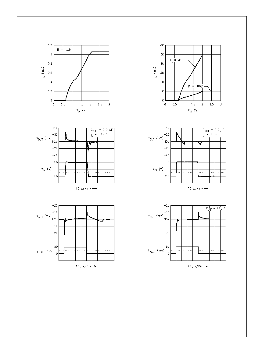
Typical Performance Characteristics
Unless otherwise specified: T
A
= 25∞C, C
OUT
= 4.7 µF,
C
IN
= 1µF, ON/OFF pin tied to V
IN
, V
IN
= V
O(NOM)
+ 1V, V
OUT(NOM)
= 1.8V. (Continued)
Input Current vs V
IN
Input Current vs V
IN
10109110
10109111
Line Transient
Line Transient
10109124
10109125
Load Transient Response
Load Transient Response
10109114
10109115
LP2980L
V
www.national.com
7
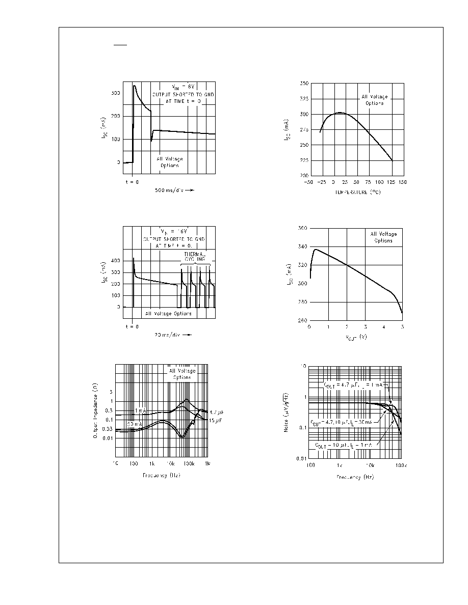
Typical Performance Characteristics
Unless otherwise specified: T
A
= 25∞C, C
OUT
= 4.7 µF,
C
IN
= 1µF, ON/OFF pin tied to V
IN
, V
IN
= V
O(NOM)
+ 1V, V
OUT(NOM)
= 1.8V. (Continued)
Short Circuit Current
Instantaneous Short Circuit Current vs
Temperature
10109126
10109127
Short Circuit Current
Instantaneous Short Circuit Current vs
Output Voltage
10109128
10109129
Output Impedance vs Frequency
Output Noise Density
10109106
10109113
LP2980L
V
www.national.com
8
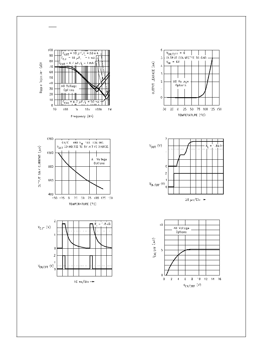
Typical Performance Characteristics
Unless otherwise specified: T
A
= 25∞C, C
OUT
= 4.7 µF,
C
IN
= 1µF, ON/OFF pin tied to V
IN
, V
IN
= V
O(NOM)
+ 1V, V
OUT(NOM)
= 1.8V. (Continued)
Ripple Rejection
Input to Output Leakage vs
Temperature
10109112
10109130
Output Reverse Leakage vs
Temperature
Turn-On Waveform
10109131
10109116
Turn-Off Waveform
ON/OFF Pin current vs V
ON/OFF
10109117
10109132
Application Hints
INPUT CAPACITOR
An input capacitor whose capacitance is
1 µF is required
between the LP2980 input pin and ground (the amount of
capacitance may be increased without limit).
The input capacitor must be located a distance of not more
than 1 cm away from the input pin and returned to a clean
analog ground. Any good quality ceramic, Tantalum, or film
capacitor may be used at the input.
IMPORTANT: Tantalum capacitors may suffer catastrophic
failure due to surge current when connected to a
low-impedance source of power (like a battery or very large
LP2980L
V
www.national.com
9
Application Hints
(Continued)
capacitor). If a Tantalum input capacitor is used, it must be
guaranteed by the manufacturer to have a surge current
rating sufficient for the application.
There are no requirements for ESR on the input capacitor,
but tolerance and temperature coefficient must be consid-
ered when selecting the capacitor to ensure the capacitance
will be
1 µF over the entire operating range.
OUTPUT CAPACITOR
The LP2980 requires an output capacitor to maintain loop
stability. The capacitor must be selected to meet the require-
ments of capacitance and ESR (equivalent series resis-
tance) over the full operating temperature range of the ap-
plication (see SELECTING THE OUTPUT CAPACITOR).
The minimum amount of capacitance which can be used on
the output is 2.2 µF, but this value may be increased without
limit.
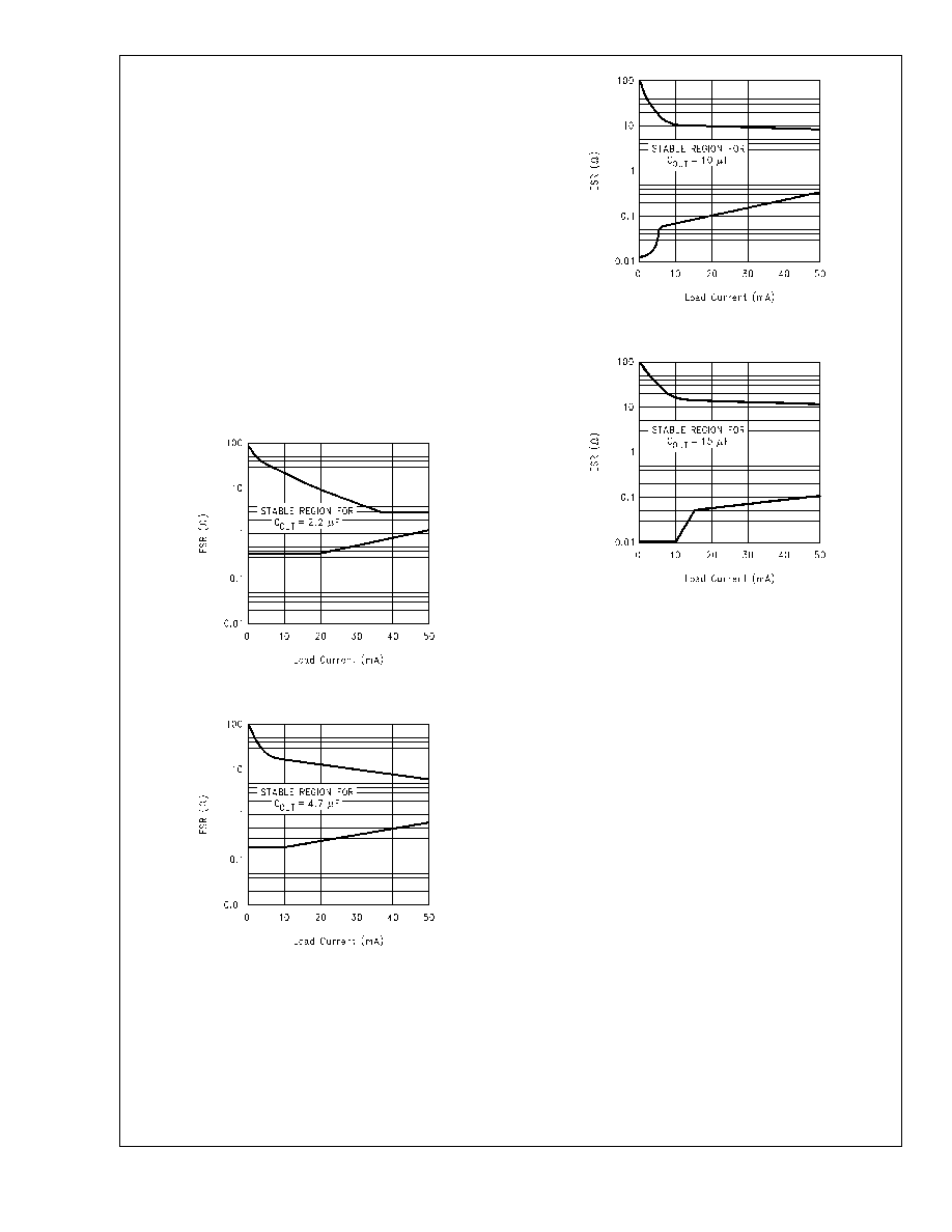
Four curves are provided which show the stable ESR range
of the LP2980-1.8V operated with output capacitances of
2.2, 4.7, 10, and 15 µF:
10109118
2.2 µF ESR Curves For 1.8V Output
10109119
4.7 µF ESR Curves For 1.8V Output
10109120
10 µF ESR Curves For 1.8V Output
10109121
15 µF ESR Curves For 1.8V Output
It should be noted that for the lower values of the output
capacitance (
<
10 µF), it may be necessary to use a capaci-
tor and series resistance to provide sufficient ESR. To un-
derstand why this is true, the basic characteristics of capaci-
tance types must be explained:
CAPACITOR CHARACTERISTICS:
Ceramic Capacitors have an extremely low ESR (in the
range of 5-15 m
), and can only be used on the output of the
LP2980 if an external resistor is placed in series to supply
the needed ESR (a resistance value of about 2
+/- 30% is
recommended).
Be careful of the temperature coefficient of ceramics: select
X7R or X5R if possible, because those types typically vary
less than +/- 25% over the range of -40 to +125∞C. Z5U
types are worse, and will typically lose half (or more) of their
capacitance over the same temperature range.
A source for large-value ceramics with good performance is
Taiyo-Yuden. Their web address is :
http://www.t-yuden.com/hicap.html
Tantalum capacitors have ESR values that are more diffi-
cult to determine: the manufacturers specify only a maxi-
mum limit, which is typically 10X or 20X the typical value.
ESR values can vary considerably from lot to lot and from
manufacturer to manufacturer. For example, some 4.7
µF/10V devices tested showed typical values in the range of
0.5 - 1
, but values as high as 6
have been seen.
It should also be noted that the ESR typically increases
about 2X - 3X when going from +125∞C down to -40∞C.
LP2980L
V
www.national.com
10

Application Hints
(Continued)
Another factor to consider is that Tantalum manufacturers
are presently designing their products toward the goal of
getting the lowest possible ESR, in an attempt to compete
with the new high-value ceramic capacitors. This means that
the typical values will probably continue to decline in the
future.
SELECTING THE OUTPUT CAPACITOR
This section contains guidelines for selecting an output ca-
pacitor which will maintain good regulator stability over the
entire operating temperature range (refer to ESR CURVES).
2.2 µF OUTPUT CAPACITOR
The smallest output capacitor which can be used with the
LP2980-1.8 is 2.2 µF. However, care must be exercised if
this value is used because of the ESR requirement.
At load currents
25mA, the stable ESR range is approxi-
mately 0.5
to 6
. This range is probably sufficiently wide
that most 2.2 µF Tantalum capacitors would fall within it.
At higher values of load currents (using a 2.2 µF output
capacitor), the stable ESR window gets very narrow. It is
likely that a Tantalum capacitor would not be a good choice
for a design that must be robust enough for mass production.
Instead, a 2.2 µF capacitor with very low ESR (either ce-
ramic or film) should be used with a 2
external resistor
placed in series to provide the ESR.
4.7 µF OUTPUT CAPACITOR
If a 4.7 µF capacitor is used, the stable range of ESR values
for 50 mA operation is approximately 0.6
to 6
. Because of
the reduced ESR values of the new Tantalum, it is possible
to find 4.7 µF Tantalum capacitors with ESR values at or
below 0.6
. To ensure a stable design, it is recommended
that an external resistor (value about 0.5
) be added in
series with the 4.7 µF Tantalum to provide adequate mini-
mum ESR.
At values of load current
20 mA, the ESR range is wide
enough that Tantalum can be used without external resis-
tance for added ESR.
Another acceptable configuration for 50 mA operation is to
use a ceramic or film 4.7 µF capacitor (which has very low
ESR) with an external 2
resistor in series.
10 µF OUTPUT CAPACITOR
50 mA operation using a 10 µF output capacitor requires an
ESR in the range of approximately 0.4
to 7
. As stated
previously, it is possible that solid Tantalum capacitors can
be found with ESR values near to or below 0.4
. An external
resistor in series with the Tantalum (value of about 0.5
) is
recommended to assure unconditional stability.
At values of load current
20 mA, the ESR range is wide
enough that Tantalum can be used without external resis-
tance for added ESR.
Another acceptable configuration for 50 mA operation is to
use a ceramic or film 10 µF capacitor (which has very low
ESR) with an external 2
resistor in series.
15 µF OUTPUT CAPACITOR
The stable ESR range (for 50 mA load current) using a 15 µF
output capacitor is approximately 0.1
to 10
. It is ex-
tremely unlikely that a 15 µF Tantalum capacitor would be
found with an ESR below 0.1
, so no external resistance is
required with a Tantalum.
As before, another acceptable configuration for 50 mA op-
eration is to use a ceramic or film 15 µF capacitor with an
external 2
resistor in series.
ON/OFF INPUT OPERATION
The LP2980 is shut off by pulling the ON/OFF input low, and
turned on by pulling it high. If this feature is not to be used,
this pin should be tied to V
IN
to keep the regulator on at all
times.
To ensure proper operation, the signal source used to drive
the ON/OFF input must be able to swing above and below
the specified turn-on/turn-off voltage thresholds (see Electri-
cal Characteristics).
It is also important that the turn-on (and turn-off) voltage
signals applied to the ON/OFF input have a slew rate which
is not less than 40 mV/µs.
CAUTION: The regulator output state can not be guaranteed
if a slow-moving AC (or DC) signal is applied that it is in the
range between the turn-on/turn-off voltage thresholds speci-
fied in the Electrical Characteristics section.
REVERSE INPUT/OUTPUT VOLTAGE
The PNP power transistor used as the pass element in the
LP2980 has an inherent diode connected between the regu-
lator output and input. During normal operation (where the
input voltage is higher than the output) this diode is
reverse-biased.
However, if the output is pulled above the input, this diode
will turn ON and current will flow into the regulator output. In
such cases, a parasitic SCR can latch which will allow a high
current to flow into V
IN
(and out the ground pin), which can
damage the part.
In any application where the output may be pulled above the
input, an external Schottky diode must be connected from
V
IN
to V
OUT
(cathode on V
IN
, anode on V
OUT
), to limit the
reverse voltage across the LP2980 to 0.3V (see Basic Ap-
plication Circuit).
LP2980L
V
www.national.com
11
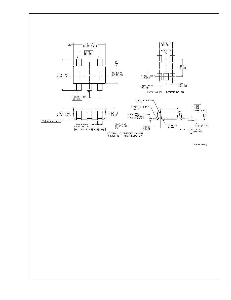
Physical Dimensions
inches (millimeters)
unless otherwise noted
5-Lead Small Outline Package (M5)
NS Package Number MF05A
For Order Numbers, refer to
Table 1 in the "Order Information" section of this document.
LP2980L
V
www.national.com
12
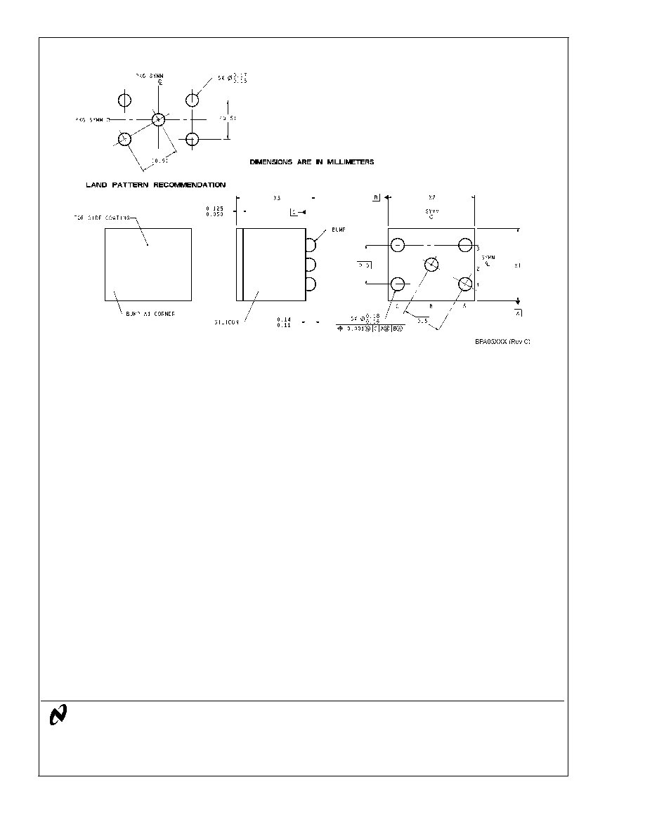
Physical Dimensions
inches (millimeters) unless otherwise noted (Continued)
micro SMD, 5 Bump, Package (BPA05)
NS Package Number BPA05A
For Order Numbers, refer to
Table 1in the "Ordering Information" section of this document.
The dimensions for X1, X2 and X3 are as given:
X1 = 0.930 +/- 0.030mm
X2 = 1.107 +/- 0.030mm
X3 = 0.850 +/- 0.050mm
NOTES: UNLESS OTHERWISE SPECIFIED
1. EPOXY COATING
2. 63Sn/37Pb EUTECTIC BUMP
3. RECOMMEND NON-SOLDER MASK DEFINED LANDING PAD.
4. PIN 1 IS ESTABLISHED BY LOWER LEFT CORNER WITH RESPECT TO TEXT ORIENTATION. REMAINING PINS ARE NUMBERED COUNTER
CLOCKWISE.
5. XXX IN DRAWING NUMBER REPRESENTS PACKAGE SIZE VARIATION WHERE X1 IS PACKAGE WIDTH, X2 IS PACKAGE LENGTH AND X3 IS
PACKAGE HEIGHT.
6.NO JEDEC REGISTRATION AS OF AUG.1999.
LIFE SUPPORT POLICY
NATIONAL'S PRODUCTS ARE NOT AUTHORIZED FOR USE AS CRITICAL COMPONENTS IN LIFE SUPPORT
DEVICES OR SYSTEMS WITHOUT THE EXPRESS WRITTEN APPROVAL OF THE PRESIDENT AND GENERAL
COUNSEL OF NATIONAL SEMICONDUCTOR CORPORATION. As used herein:
1. Life support devices or systems are devices or
systems which, (a) are intended for surgical implant
into the body, or (b) support or sustain life, and
whose failure to perform when properly used in
accordance with instructions for use provided in the
labeling, can be reasonably expected to result in a
significant injury to the user.
2. A critical component is any component of a life
support device or system whose failure to perform
can be reasonably expected to cause the failure of
the life support device or system, or to affect its
safety or effectiveness.
National Semiconductor
Corporation
Americas
Email: support@nsc.com
National Semiconductor
Europe
Fax: +49 (0) 180-530 85 86
Email: europe.support@nsc.com
Deutsch Tel: +49 (0) 69 9508 6208
English
Tel: +44 (0) 870 24 0 2171
FranÁais Tel: +33 (0) 1 41 91 8790
National Semiconductor
Asia Pacific Customer
Response Group
Tel: 65-2544466
Fax: 65-2504466
Email: ap.support@nsc.com
National Semiconductor
Japan Ltd.
Tel: 81-3-5639-7560
Fax: 81-3-5639-7507
www.national.com
LP2980L
V
Micropower
SOT
,
5
0
m
A
Low-V
oltage
Low-Dropout
Regulator
For
Applications
W
ith
Output
V
oltages
<
2V
National does not assume any responsibility for use of any circuitry described, no circuit patent licenses are implied and National reserves the right at any time without notice to change said circuitry and specifications.