LP2980-ADJ
Micropower SOT, 50 mA Ultra Low-Dropout Adjustable
Voltage Regulator
General Description
The LP2980-ADJ is a 50 mA adjustable voltage regulator de-
signed to provide ultra low dropout in battery powered appli-
cations.
Using an optimized VIP
TM
(vertically Integrated PNP) pro-
cess, the LP2980-ADJ delivers unequalled performance in
all specifications critical to battery-powered designs:
Adjustable Output: output voltage can be set from 1.23V to
15V.
Precision Reference: 0.75% tolerance.
Dropout Voltage: typically 120 mV
@
50 mA load, and 7 mV
@
1 mA load.
Ground Pin Current: typically 320 µA
@
50 mA load, and 80
µA
@
1 mA load.
Sleep Mode: less than 1 µA quiescent current when on/off
pin is pulled low.
Smallest Possible Size: SOT-23 package uses minimum
board space.
Features
n
Ultra low dropout voltage
n
Output adjusts from 1.23V to 15V
n
Guaranteed 50 mA output current
n
Uses tiny SOT-23 package
n
Requires few external components
n
<
1 µA quiescent current when shutdown
n
Low ground pin current at all loads
n
High peak current capability (150 mA typical)
n
Wide supply voltage range (2.5V≠16V)
n
Overtemperature/overcurrent protection
n
-40∞C to +125∞C Junction temperature range
Applications
n
Cellular Phone
n
Palmtop/Laptop Computer
n
Camcorder, Personal Stereo, Camera
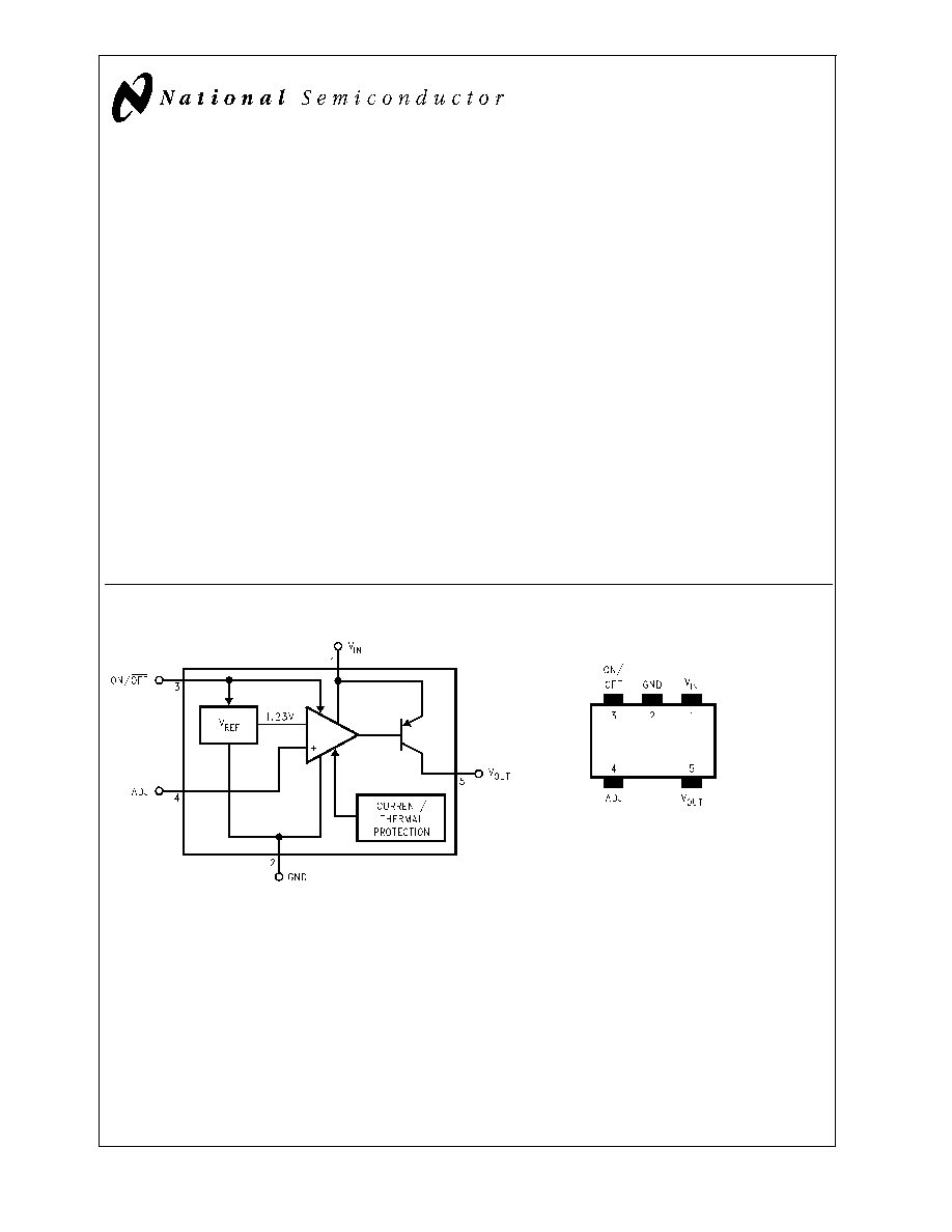
Block Diagram
Connection Diagram
VIP
TM
is a trademark of National Semiconductor Corporation.
DS100001-1
5-Lead Small Outline Package (M5)
DS100001-2
Top View
See NS Package Number MA05B
For ordering Information, refer to
Table 1 in this
document
April 2000
LP2980-ADJ
Micropower
SOT
,
5
0
m
A
Ultra
Low-Dropout
Adjustable
V
oltage
Regulator
© 2000 National Semiconductor Corporation
DS100001
www.national.com
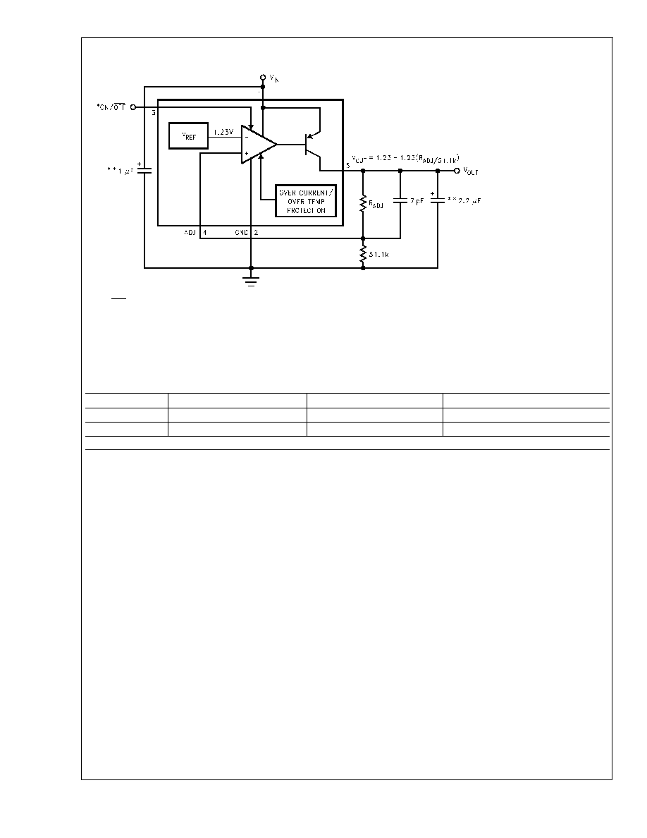
Basic Application Circuit
Ordering Information
TABLE 1. Package Marking and Ordering Information
Grade
Order Information
Package Marking
Supplied as
STD
LP2980IM5X-ADJ
L06B
3k Units on Tape and Reel
STD
LP2980IM5-ADJ
L06B
250 Units on Tape and Reel
For fixed output voltage versions, see LP2980 and LP2980LV datasheets.
DS100001-3
*ON/OFF INPUT MUST BE ACTIVELY TERMINATED. TIE TO V
IN
IF THIS
FUNCTION IS NOT TO BE USED.
**MINIMUM CAPACITANCE IS SHOWN TO ENSURE STABILITY OVER
FULL LOAD CURRENT RANGE (SEE APPLICATION HINTS).
LP2980-ADJ
www.national.com
2
Absolute Maximum Ratings
(Note 1)
If Military/Aerospace specified devices are required, please contact the National Semiconductor Sales Office/
Distributors for availability and specifications.
Storage Temperature Range
-65 to +150∞C
Operating Junction Temperature
Range
-40 to +125∞C
Lead Temp. (Soldering, 5 seconds)
260∞C
ESD Rating (Note 2)
2 kV
Power Dissipation (Note 3)
Internally Limited
Input Supply Voltage (Survival)
-0.3V to +16V
Input Supply Voltage (Operating)
2.5V to +16V
Shutdown Input Voltage (Survival)
-0.3V to +16V
Output Voltage (Survival) (Note 4)
-0.3V to 16V
I
OUT
(Survival)
Short Circuit Protected
Input-Output Voltage (Survival)
(Note 5)
-0.3V to 16V
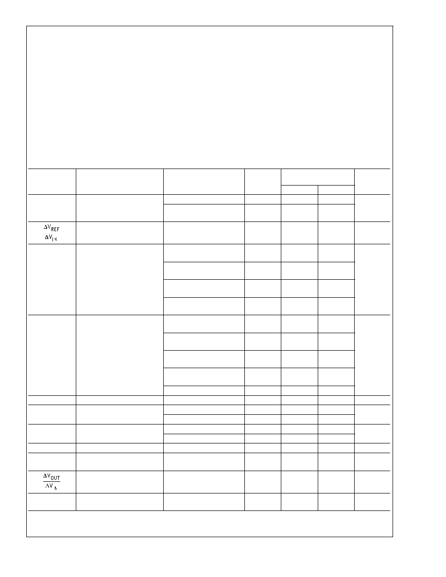
Electrical Characteristics
Limits in standard typeface are for T
J
= 25∞C, and limits in boldface type apply over the full operating temperature range.
Unless otherwise specified: V
IN
= 4.3V, V
OUT
= 3.3V, I
L
= 1 mA, C
IN
= 1 µF, C
OUT
= 2.2 µF, V
ON/OFF
= 2V.
Symbol
Parameter
Conditions
Typ
LP2980I-ADJ (Note
6)
Units
Min
Max
V
REF
Reference Voltage
1.225
1.213
1.237
V
1 mA
<
I
L
<
50 mA
V
OUT
+ 1
V
IN
16V
1.225
1.206
1.182
1.243
1.268
Reference Voltage Line
Regulation
2.5V
V
IN
16V
3
6.0
15.0
mV
V
IN
≠V
O
Dropout Voltage (Note 7)
I
L
= 0
1
3
5
mV
I
L
= 1 mA
7
10
15
I
L
= 10 mA
40
60
90
I
L
= 50 mA
120
150
225
I
GND
Ground Pin Current
I
L
= 0
60
95
125
µA
I
L
= 1 mA
80
110
170
I
L
= 10 mA
120
220
460
I
L
= 50 mA
320
600
1200
V
ON/OFF
<
0.18V
0.01
1
I
ADJ
ADJ Pin Bias Current
1 mA
I
L
50 mA
150
350
nA
V
ON/OFF
ON/OFF Input Voltage
(Note 8)
High = O/P ON
1.4
1.6
V
Low = O/P OFF
0.55
0.18
I
ON/OFF
ON/OFF Input Current
V
ON/OFF
= 0
0.01
-1
µA
V
ON/OFF
= 5V
5
15
I
O
(PK)
Peak Output Current
V
OUT
V
O
(NOM) - 5%
150
100
mA
e
n
Output Noise Voltage
(RMS)
BW = 300 Hz to 50 kHz,
C
OUT
= 10 µF
160
µV
Ripple Rejection
f = 1 kHz
C
OUT
= 10 µF
68
dB
I
O
(MAX)
Short Circuit Current
R
L
= 0 (Steady State)
(Note 9)
150
mA
LP2980-ADJ
www.national.com
3
Electrical Characteristics
(Continued)
Note 1: Absolute maximum ratings indicate limits beyond which damage to the component may occur. Electrical specifications do not apply when operating the de-
vice outside of its rated operating conditions.
Note 2: The ESD rating of pins 3 and 4 is 1 kV.
Note 3: The maximum allowable power dissipation is a function of the maximum junction temperature, T
J
(MAX), the junction-to-ambient thermal resistance,
J-A
, and
the ambient temperature, T
A
. The maximum allowable power dissipation at any ambient temperature is calculated using:
The value of
J-A
for the SOT-23 package is 300∞C/W. Exceeding the maximum allowable power dissipation will cause excessive die temperature, and the regulator
will go into thermal shutdown.
Note 4: If used in a dual-supply system where the regulator load is returned to a negative supply, the LP2980-ADJ output must be diode-clamped to ground.
Note 5: The output PNP structure contains a diode between the V
IN
and V
OUT
terminals that is normally reverse-biased. Reversing the polarity from V
IN
to V
OUT
will turn on this diode (see Application Hints).
Note 6: Limits are 100% production tested at 25∞C. Limits over the operating temperature range are guaranteed through correlation using Statistical Quality Control
(SQC) methods. The limits are used to calculate National's Average Outgoing Quality Level (AOQL).
Note 7: Dropout voltage is defined as the input to output differential at which the output voltage drops 100 mV below the value measured with a 1V differential.
Note 8: The ON/OFF input must be properly driven to prevent possible misoperation. For details, refer to Application Hints.
Note 9: See Typical Performance Characteristics curves.
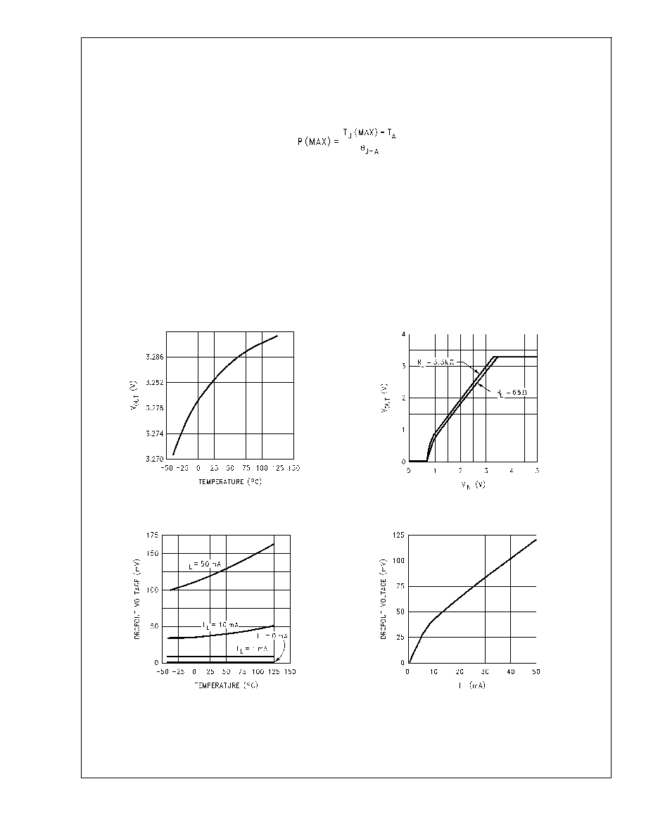
Typical Performance Characteristics
Unless otherwise specified: T
A
= 25∞C, V
IN
= V
O
(NOM) + 1V,
I
L
= 1 mA, ON/OFF pin tied to V
IN
, R
ADJ
= 86.6k, and test circuit is as shown in Basic Application Circuit.
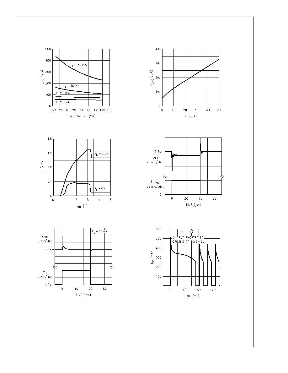
Output Voltage vs. Temperature
DS100001-5
Dropout Characteristics
DS100001-6
Dropout Voltage vs. Temperature
DS100001-7
Dropout Voltage vs. Load Current
DS100001-8
LP2980-ADJ
www.national.com
4
Typical Performance Characteristics
Unless otherwise specified: T
A
= 25∞C, V
IN
= V
O
(NOM) + 1V,
I
L
= 1 mA, ON/OFF pin tied to V
IN
, R
ADJ
= 86.6k, and test circuit is as shown in Basic Application Circuit. (Continued)
Ground Pin Current vs. Temperature
DS100001-9
Ground Pin Current vs. Load Current
DS100001-10
Input Current vs. V
IN
DS100001-11
Load Transient Response
DS100001-12
Line Transient Response
DS100001-13
Short Circuit Current
DS100001-14
LP2980-ADJ
www.national.com
5