LP2982
Micropower 50 mA Ultra Low-Dropout Regulator in
SOT-23 and micro SMD Packages
General Description
The LP2982 is a 50 mA, fixed-output voltage regulator de-
signed to provide ultra low dropout and lower noise in battery
powered applications.
Using an optimized VIP
TM
(Vertically Integrated PNP) pro-
cess, the LP2982 delivers unequaled performance in all
specifications critical to battery-powered designs:
Dropout Voltage: Typically 120 mV
@
50 mA load, and 7 mV
@
1 mA load.
Ground Pin Current: Typically 375 µA
@
50 mA load, and
80 µA
@
1 mA load.
Sleep Mode: Less than 1 µA quiescent current when on/off
pin is pulled low.
Smallest Possible Size: SOT-23 and micro SMD packages
use absolute minimum board space.
Precision Output: 1.0% tolerance output voltages available
(A grade).
Low Noise: By adding an external bypass capacitor, output
noise can be reduced to 30 µV (typical).
Ten output voltage versions, from 2.5V to 5.0V, are available
as standard products.
Features
n
Ultra low dropout voltage
n
Guaranteed 50 mA output current
n
Typical dropout voltage 180 mV
@
80 mA
n
Smallest possible size (SOT-23, micro SMD package)
n
Requires minimum external components
n
<
1 µA quiescent current when shutdown
n
Low ground pin current at all loads
n
Output voltage accuracy 1.0% (A Grade)
n
High peak current capability (150 mA typical)
n
Wide supply voltage range (16V max)
n
Low Z
OUT
0.3
typical (10 Hz to 1 MHz)
n
Overtemperature/overcurrent protection
n
-40∞C to +125∞C junction temperature range
n
Custom voltages available
Applications
n
Cellular Phone
n
Palmtop/Laptop Computer
n
Personal Digital Assistant (PDA)
n
Camcorder, Personal Stereo, Camera
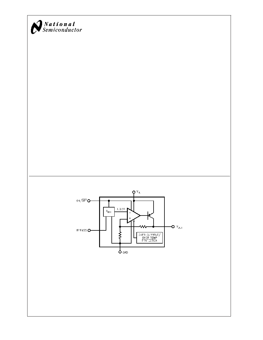
Block Diagram
01267901
VIP
TM
is a trademark of National Semiconductor Corporation.
January 2003
LP2982
Micropower
50
mA
Ultra
Low-Dropout
Regulator
in
SOT
-23
and
micro
SMD
Packages
© 2003 National Semiconductor Corporation
DS012679
www.national.com
Connection Diagrams
5-Lead Small Outline Package (M5)
micro SMD, 5 Bump Package (BPA05)
01267903
Top View
See NS Package Number MF05A
For ordering information see Table 1
01267957
Note: The actual physical placement of the package marking will vary from
part to part. Package marking contains date code and lot traceability
information, and will vary considerably. Package marking does not correlate
to device type.
Top View
See NS Package Number BPA05
Pin Descrption
Name
Pin Number
Function
SOT-23
micro SMD
V
IN
1
C3
Input Voltage
GND
2
A1
Common Ground (device substrate)
ON/OFF
3
A3
Logic high enable input
BYPASS
4
B2
Bypass capacitor for low noise operation
V
OUT
5
C1
Regulated output voltage
Basic Application Circuit
01267902
*ON/OFF input must be actively terminated. Tie to V
IN
if this function is not to be used.
**Minimum capacitance is shown to insure stability over full load current range. More capacitance provides superior dynamic performance (see Application
Hints).
***See Application Hints.
LP2982
www.national.com
2

Ordering Information
TABLE 1. Package Marking and Ordering Information
Output Voltage
(V)
Grade
Order Information
Package
Marking
Supplied as:
5-Lead Small Outline Package (M5)
2.5
A
LP2982AIM5X-2.5
L58A
3000 Units on Tape and Reel
2.5
A
LP2982AIM5-2.5
L58A
1000 Units on Tape and Reel
2.5
STD
LP2982IM5X-2.5
L58B
3000 Units on Tape and Reel
2.5
STD
LP2982IM5-2.5
L58B
1000Units on Tape and Reel
2.6
A
LP2982AIM5X-2.6
LBYA
3000 Units on Tape and Reel
2.6
A
LP2982AIM5-2.6
LBYA
1000 Units on Tape and Reel
2.6
STD
LP2982IM5X-2.6
LBYB
3000 Units on Tape and Reel
2.6
STD
LP2982IM5-2.6
LBYB
1000Units on Tape and Reel
2.8
A
LP2982AIM5X-2.8
L60A
3000 Units on Tape and Reel
2.8
A
LP2982AIM5-2.8
L60A
1000 Units on Tape and Reel
2.8
STD
LP2982IM5X-2.8
L60B
3000 Units on Tape and Reel
2.8
STD
LP2982IM5-2.8
L60B
1000 Units on Tape and Reel
3.0
A
LP2982AIM5X-3.0
L20A
3000 Units on Tape and Reel
3.0
A
LP2982AIM5-3.0
L20A
1000 Units on Tape and Reel
3.0
STD
LP2982IM5X-3.0
L20B
3000 Units on Tape and Reel
3.0
STD
LP2982IM5-3.0
L20B
1000 Units on Tape and Reel
3.3
A
LP2982AIM5X-3.3
L19A
3000 Units on Tape and Reel
3.3
A
LP2982AIM5-3.3
L19A
1000 Units on Tape and Reel
3.3
STD
LP2982IM5X-3.3
L19B
3000 Units on Tape and Reel
3.3
STD
LP2982IM5-3.3
L19B
1000 Units on Tape and Reel
3.6
A
LP2982AIM5X-3.6
L0BA
3000 Units on Tape and Reel
3.6
A
LP2982AIM5-3.6
L0BA
1000 Units on Tape and Reel
3.6
STD
LP2982IM5X-3.6
L0BB
3000 Units on Tape and Reel
3.6
STD
LP2982IM5-3.6
L0BB
1000 Units on Tape and Reel
3.8
A
LP2982AIM5X-3.8
L76A
3000 Units on Tape and Reel
3.8
A
LP2982AIM5-3.8
L76A
1000 Units on Tape and Reel
3.8
STD
LP2982IM5X-3.8
L76B
3000 Units on Tape and Reel
3.8
STD
LP2982IM5-3.8
L76B
1000 Units on Tape and Reel
4.0
A
LP2982AIM5X-4.0
L29A
3000 Units on Tape and Reel
4.0
A
LP2982AIM5-4.0
L29A
1000 Units on Tape and Reel
4.0
STD
LP2982IM5X-4.0
L29B
3000 Units on Tape and Reel
4.0
STD
LP2982IM5-4.0
L29B
1000 Units on Tape and Reel
4.5
A
LP2982AIM5X-4.5
LA8A
3000 Units on Tape and Reel
4.5
A
LP2982AIM5-4.5
LA8A
1000 Units on Tape and Reel
4.5
STD
LP2982IM5X-4.5
LA8B
3000 Units on Tape and Reel
4.5
STD
LP2982IM5-4.5
LA8B
1000 Units on Tape and Reel
4.7
A
LP2982AIM5X-4.7
L0HA
3000 Units on Tape and Reel
4.7
A
LP2982AIM5-4.7
L0HA
1000 Units on Tape and Reel
4.7
STD
LP2982IM5X-4.7
L0HB
3000 Units on Tape and Reel
4.7
STD
LP2982IM5-4.7
L0HB
1000 Units on Tape and Reel
5.0
A
LP2982AIM5X-5.0
L18A
3000 Units on Tape and Reel
5.0
A
LP2982AIM5-5.0
L18A
1000 Units on Tape and Reel
5.0
STD
LP2982IM5X-5.0
L18B
3000 Units on Tape and Reel
5.0
STD
LP2982IM5-5.0
L18B
1000 Units on Tape and Reel
5.3
A
LP2982AIM5X-5.3
LBZA
3000 Units on Tape and Reel
5.3
A
LP2982AIM5-5.3
LBZA
1000 Units on Tape and Reel
LP2982
www.national.com
3
Ordering Information
(Continued)
TABLE 1. Package Marking and Ordering Information (Continued)
Output Voltage
(V)
Grade
Order Information
Package
Marking
Supplied as:
5.3
STD
LP2982IM5X-5.3
LBZB
3000 Units on Tape and Reel
5.3
STD
LP2982IM5-5.3
LBZB
1000 Units on Tape and Reel
micro SMD, 5 Bump Package (BPA05)
2.8
A
LP2982AIBP-2.8
250 Units on Tape and Reel
2.8
A
LP2982AIBPX-2.8
3000 Units on Tape and Reel
2.8
STD
LP2982IBP-2.8
250 Units on Tape and Reel
2.8
STD
LP2982IBPX-2.8
3000 Units on Tape and Reel
3.0
A
LP2982AIBP-3.0
250 Units on Tape and Reel
3.0
A
LP2982AIBPX-3.0
3000 Units on Tape and Reel
3.0
STD
LP2982IBP-3.0
250 Units on Tape and Reel
3.0
STD
LP2982IBPX-3.0
3000 Units on Tape and Reel
LP2982
www.national.com
4
Absolute Maximum Ratings
(Note 1)
If Military/Aerospace specified devices are required,
please contact the National Semiconductor Sales Office/
Distributors for availability and specifications.
Storage Temperature Range
-65∞C to +150∞C
Operating Junction Temperature Range -40∞C to +125∞C
Lead Temperature (Soldering, 5
sec.)
260∞C
ESD Rating (Note 2)
2 kV
Power Dissipation (Note 3)
Internally Limited
Input Supply Voltage (Survival)
-0.3V to +16V
Input Supply Voltage (Operating)
2.1V to +16V
Shutdown Input Voltage (Survival)
-0.3V to +16V
Output Voltage (Survival, (Note 4))
-0.3V to +9V
I
OUT
(Survival)
Short Circuit Protected
Input-Output Voltage (Survival, (Note 5))
-0.3V to +16V
Electrical Characteristics
(Note 10)
Limits in standard typeface are for T
J
= 25∞C, and limits in boldface type apply over the full operating temperature range. Un-
less otherwise specified: V
IN
= V
O(NOM)
+ 1V, I
L
= 1 mA, C
IN
= 1 µF, C
OUT
= 4.7 µF, V
ON/OFF
= 2V.
Symbol
Parameter
Conditions
Typ
LP2982AI-X.X
LP2982I-X.X
Units
(Note 6)
(Note 6)
Min
Max
Min
Max
V
O
Output Voltage
Tolerance
I
L
= 1 mA
-1.0
+1.0
-1.5
+1.5
%V
NOM
1 mA
<
I
L
<
50 mA
-1.5
+1.5
-2.0
+2.0
-2.0
+2.0
-3.5
+3.5
Output Voltage Line
Regulation
V
O(NOM)
+ 1V
V
IN
16V
0.007
0.014
0.014
%/V
0.032
0.032
V
IN
≠V
O
Dropout Voltage
I
L
= 0
1
3
3
mV
(Note 7)
5
5
I
L
= 1 mA
7
10
10
15
15
I
L
= 10 mA
40
60
60
90
90
I
L
= 50 mA
120
150
150
225
225
I
GND
Ground Pin Current
I
L
= 0
65
95
95
µA
125
125
I
L
= 1 mA
80
110
110
170
170
I
L
= 10 mA
140
220
220
460
460
I
L
= 50 mA
375
600
600
1200
1200
V
ON/OFF
<
0.3V
0.01
0.8
0.8
V
ON/OFF
<
0.15V
0.10
2.0
2.0
V
ON/OFF
ON/OFF Input Voltage
High = O/P ON
1.4
1.6
1.6
V
(Note 8)
Low = O/P OFF
0.55
0.15
0.15
I
ON/OFF
ON/OFF Input Current
V
ON/OFF
= 0
0.01
-2
-2
µA
V
ON/OFF
= 5V
5
15
15
I
O(PK)
Peak Output Current
V
OUT
V
O(NOM)
- 5%
150
100
100
mA
V
IN
≠V
O
Dropout Voltage
I
L
= 80 mA
180
225
225
mV
325
325
I
GND
Ground Pin Current
I
L
= 80 mA
525
750
750
µA
1400
1400
e
n
Output Noise Voltage
(RMS)
BW = 300 Hz≠50 kHz,
C
OUT
= 10 µF
C
BYPASS
= 0.01 µF
30
µV
LP2982
www.national.com
5