LP2986
Micropower, 200 mA Ultra Low-Dropout Fixed or
Adjustable Voltage Regulator
General Description
The LP2986 is a 200 mA precision LDO voltage regulator
which offers the designer a higher performance version of
the industry standard LP2951.
Using an optimized VIP
TM
(Vertically Integrated PNP) pro-
cess, the LP2986 delivers superior performance:
Dropout Voltage: Typically 180 mV
@
200 mA load, and 1
mV
@
1 mA load.
Ground Pin Current: Typically 1 mA
@
200 mA load, and
200 µA
@
10 mA load.
Sleep Mode: The LP2986 draws less than 1 µA quiescent
current when shutdown pin is pulled low.
Error Flag: The built-in error flag goes low when the output
drops approximately 5% below nominal.
Precision Output: The standard product versions available
can be pin-strapped (using the internal resistive divider) to
provide output voltages of 5.0V, 3.3V, or 3.0V with guaran-
teed accuracy of 0.5% ("A" grade) and 1% (standard grade)
at room temperature.
Features
n
Ultra low dropout voltage
n
Guaranteed 200 mA output current
n
SO-8 and mini-SO8 surface mount packages
n
<
1 µA quiescent current when shutdown
n
Low ground pin current at all loads
n
0.5% output voltage accuracy ("A" grade)
n
High peak current capability (400 mA typical)
n
Wide supply voltage range (16V max)
n
Overtemperature/overcurrent protection
n
-40∞C to +125∞C junction temperature range
Applications
n
Cellular Phone
n
Palmtop/Laptop Computer
n
Camcorder, Personal Stereo, Camera
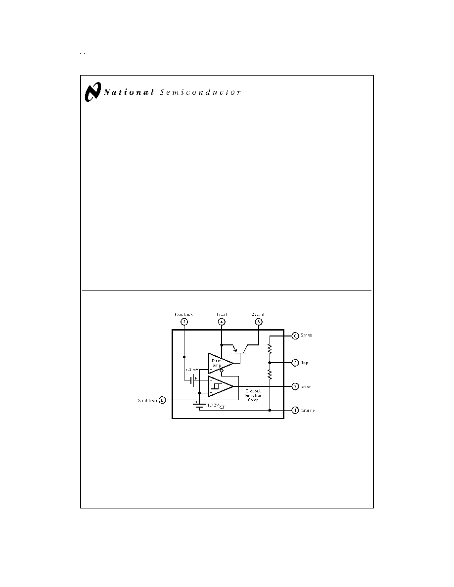
Block Diagram
VIP
TM
is a trademark of National Semiconductor Corporation.
DS012935-1
March 1999
LP2986
Micropower
,
200
mA
Ultra
Low-Dropout
Fixed
or
Adjustable
V
oltage
Regulator
© 1999 National Semiconductor Corporation
DS012935
www.national.com
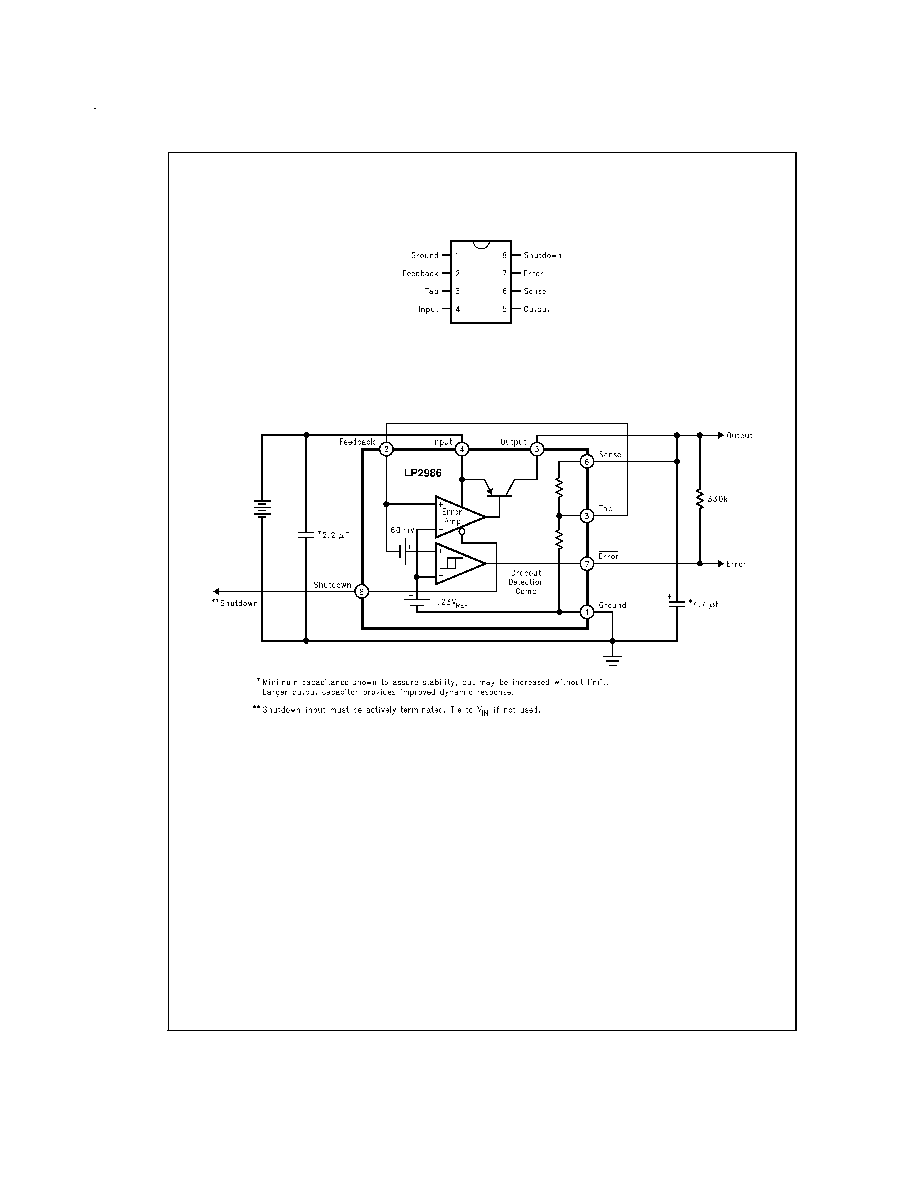
Connection Diagram and Ordering Information
Basic Application Circuits
Surface Mount Packages:
Mini SO-8 Package Type MM: See NS Package Drawing Number MUA08A
SO-8 Package Type M: See NS Package Drawing Number M08A
DS012935-2
Top View
For ordering information, refer to Table 1 of this document.
Application Using Internal Resistive Divider
DS012935-3
www.national.com
2
Basic Application Circuits
(Continued)
Ordering Information
TABLE 1. Package Marking and Ordering Information
Output Voltage
Grade
Order Information
Package Marking
Supplied as:
5
A
LP2986AIMMX-5.0
L41A
3.5k Units on Tape and Reel
5
A
LP2986AIMM-5.0
L41A
250 Units on Tape and Reel
5
STD
LP2986IMMX-5.0
L41B
3.5k Units on Tape and Reel
5
STD
LP2986IMM-5.0
L41B
250 Units on Tape and Reel
3.3
A
LP2986AIMMX-3.3
L40A
3.5k Units on Tape and Reel
3.3
A
LP2986AIMM-3.3
L40A
250 Units on Tape and Reel
3.3
STD
LP2986IMMX-3.3
L40B
3.5k Units on Tape and Reel
3.3
STD
LP2986IMM-3.3
L40B
250 Units on Tape and Reel
3.0
A
LP2986AIMMX-3.0
L39A
3.5k Units on Tape and Reel
3.0
A
LP2986AIMM-3.0
L39A
250 Units on Tape and Reel
3.0
STD
LP2986IMMX-3.0
L39B
3.5k Units on Tape and Reel
3.0
STD
LP2986IMM-3.0
L39B
250 Units on Tape and Reel
5
A
LP2986AIMX-5.0
2986AIM5.0
2.5k Units on Tape and Reel
5
A
LP2986AIM-5.0
2986AIM5.0
Shipped in Anti-Static Rails
5
STD
LP2986IMX-5.0
2986IM5.0
2.5k Units on Tape and Reel
5
STD
LP2986IM-5.0
2986IM5.0
Shipped in Anti-Static Rails
3.3
A
LP2986AIMX-3.3
2986AIM3.3
2.5k Units on Tape and Reel
3.3
A
LP2986AIM-3.3
2986AIM3.3
Shipped in Anti-Static Rails
3.3
STD
LP2986IMX-3.3
2986IM3.3
2.5k Units on Tape and Reel
3.3
STD
LP2986IM-3.3
2986IM3.3
Shipped in Anti-Static Rails
3.0
A
LP2986AIMX-3.0
2986AIM3.0
2.5k Units on Tape and Reel
3.0
A
LP2986AIM-3.0
2986AIM3.0
Shipped in Anti-Static Rails
3.0
STD
LP2986IMX-3.0
2986IM3.0
2.5k Units on Tape and Reel
3.0
STD
LP2986IM-3.0
2986IM3.0
Shipped in Anti-Static Rails
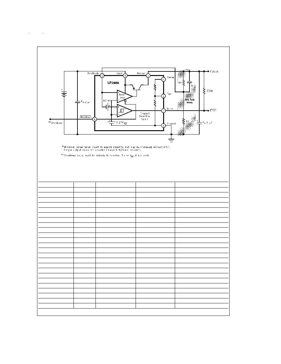
Application Using External Divider
DS012935-4
www.national.com
3
Absolute Maximum Ratings
(Note 1)
If Military/Aerospace specified devices are required,
please contact the National Semiconductor Sales Office/
Distributors for availability and specifications.
Storage Temperature Range
-65∞C to +150∞C
Operating Junction
Temperature Range
-40∞C to +125∞C
Lead Temperature
(Soldering, 5 seconds)
260∞C
ESD Rating (Note 2)
2 kV
Power Dissipation (Note 3)
Internally Limited
Input Supply Voltage
(Survival)
-0.3V to +16V
Input Supply Voltage
(Operating)
2.1V to +16V
Shutdown Pin
-0.3V to +16V
Feedback Pin
-0.3V to +5V
Output Voltage
(Survival) (Note 4)
-0.3V to +16V
I
OUT
(Survival)
Short Circuit Protected
Input-Output Voltage
(Survival) (Note 5)
-0.3V to +16V
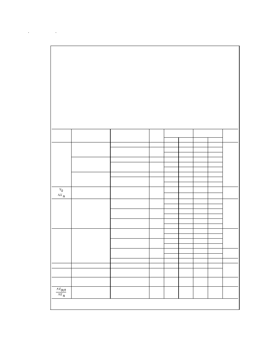
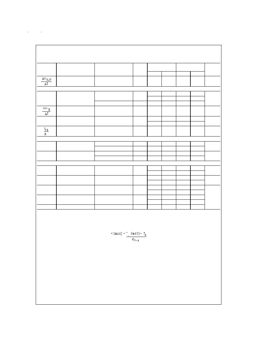
Electrical Characteristics
Limits in standard typeface are for T
J
= 25∞C, and limits in boldface type apply over the full operating temperature range. Un-
less otherwise specified: V
IN
= V
O
(NOM) + 1V, I
L
= 1 mA, C
OUT
= 4.7 µF, C
IN
= 2.2 µF, V
S/D
= 2V.
Symbol
Parameter
Conditions
Typical
LM2986AI-X.X
(Note 6)
LM2986I-X.X
(Note 6)
Units
Min
Max
Min
Max
V
O
Output Voltage
(5.0V Versions)
5.0
4.975
5.025
4.950
5.050
V
0.1 mA
<
I
L
<
200 mA
5.0
4.960
5.040
4.920
5.080
4.910
5.090
4.860
5.140
Output Voltage
(3.3V Versions)
3.3
3.283
3.317
3.267
3.333
0.1 mA
<
I
L
<
200 mA
3.3
3.274
3.326
3.247
3.353
3.241
3.359
3.208
3.392
Output Voltage
(3.0V Versions)
3.0
2.985
3.015
2.970
3.030
0.1 mA
<
I
L
<
200 mA
3.0
2.976
3.024
2.952
3.048
2.946
3.054
2.916
3.084
Output Voltage Line
Regulation
V
O
(NOM) + 1V
V
IN
16V
0.007
0.014
0.014
%/V
0.032
0.032
V
IN
≠V
O
Dropout Voltage
(Note 7)
I
L
= 100 µA
1
2.0
2.0
mV
3.5
3.5
I
L
= 75 mA
90
120
120
170
170
I
L
= 200 mA
180
230
230
350
350
I
GND
Ground Pin Current
I
L
= 100 µA
100
120
120
µA
150
150
I
L
= 75 mA
500
800
800
1400
1400
I
L
= 200 mA
1
2.1
2.1
mA
3.7
3.7
V
S/D
<
0.3V
0.05
1.5
1.5
µA
I
O
(PK)
Peak Output Current
V
OUT
V
O
(NOM) - 5%
400
250
250
mA
I
O
(MAX)
Short Circuit Current
R
L
= 0 (Steady State)
(Note 11)
400
e
n
Output Noise Voltage
(RMS)
BW = 300 Hz to 50
kHz, C
OUT
= 10 µF
160
µV(RMS)
Ripple Rejection
f = 1 kHz, C
OUT
= 10 µF
65
dB
www.national.com
4
Electrical Characteristics
(Continued)
Limits in standard typeface are for T
J
= 25∞C, and limits in boldface type apply over the full operating temperature range. Un-
less otherwise specified: V
IN
= V
O
(NOM) + 1V, I
L
= 1 mA, C
OUT
= 4.7 µF, C
IN
= 2.2 µF, V
S/D
= 2V.
Symbol
Parameter
Conditions
Typical
LM2986AI-X.X
(Note 6)
LM2986I-X.X
(Note 6)
Units
Min
Max
Min
Max
Output Voltage
Temperature Coefficient
(Note 9)
20
ppm/∞C
FEEDBACK PIN
V
FB
Feedback Pin Voltage
1.23
1.21
1.25
1.20
1.26
V
1.20
1.26
1.19
1.27
(Note 10)
1.23
1.19
1.28
1.18
1.29
FB Pin Voltage
Temperature Coefficient
(Note 9)
20
ppm/∞C
I
FB
Feedback Pin Bias
Current
I
L
= 200 mA
150
330
330
nA
760
760
FB Pin Bias Current
Temperature Coefficient
(Note 9)
0.1
nA/∞C
SHUTDOWN INPUT
V
S/D
S/D Input Voltage
(Note 8)
V
H
= O/P ON
1.4
1.6
1.6
V
V
L
= O/P OFF
0.55
0.18
0.18
I
S/D
S/D Input Current
V
S/D
= 0
0
-1
-1
µA
V
S/D
= 5V
5
15
15
ERROR COMPARATOR
I
OH
Output "HIGH" Leakage
V
OH
= 16V
0.01
1
1
µA
2
2
V
OL
Output "LOW" Voltage
V
IN
= V
O
(NOM) - 0.5V,
I
O
(COMP) = 300 µA
150
220
220
mV
350
350
V
THR
(MAX)
Upper Threshold
Voltage
-4.6
-5.5
-3.5
-5.5
-3.5
%V
OUT
-7.7
-2.5
-7.7
-2.5
V
THR
(MIN)
Lower Threshold
Voltage
-6.6
-8.9
-4.9
-8.9
-4.9
-13.0
-3.3
-13.0
-3.3
HYST
Hysteresis
2.0
Note 1: Absolute Maximum Ratings indicate limits beyond which damage to the component may occur. Electrical specifications do not apply when operating the de-
vice outside of its rated operating conditions.
Note 2: The ESD rating of the Feedback pin is 500V and the Tap pin is 1.5 kV.
Note 3: The maximum allowable power dissipation is a function of the maximum junction temperature, T
J
(MAX), the junction-to-ambient thermal resistance,
J-A
,
and the ambient temperature, T
A
. The maximum allowable power dissipation at any ambient temperature is calculated using:
The value of
J-A
for the SO-8 (M) package is 160∞C/W, and the mini SO-8 (MM) package is 200∞C/W. Exceeding the maximum allowable power dissipation will cause
excessive die temperature, and the regulator will go into thermal shutdown.
Note 4: If used in a dual-supply system where the regulator load is returned to a negative supply, the LM2986 output must be diode-clamped to ground.
Note 5: The output PNP structure contains a diode between the V
IN
and V
OUT
terminals that is normally reverse-biased. Forcing the output above the input will turn
on this diode and may induce a latch-up mode which can damage the part (see Application Hints).
Note 6: Limits are 100% production tested at 25∞C. Limits over the operating temperature range are guaranteed through correlation using Statistical Quality Control
(SQC) methods. The limits are used to calculate National's Average Outgoing Quality Level (AOQL).
Note 7: Dropout voltage is defined as the input to output differential at which the output voltage drops 100 mV below the value measured with a 1V differential.
Note 8: To prevent mis-operation, the Shutdown input must be driven by a signal that swings above V
H
and below V
L
with a slew rate not less than 40 mV/µs (see
Application Hints).
Note 9: Temperature coefficient is defined as the maximum (worst-case) change divided by the total temperature range.
Note 10: V
FB
V
OUT
(V
IN
- 1), 2.5V
V
IN
16V, 100 µA
I
L
200 mA, T
J
125∞C.
Note 11: See Typical Performance Characteristics curves.
www.national.com
5