LP2987/LP2988
Micropower, 200 mA Ultra Low-Dropout Voltage
Regulator with Programmable Power-On Reset Delay;
Low Noise Version Available (LP2988)
General Description
The LP2987/8 are fixed-output 200 mA precision LDO volt-
age regulators with power-ON reset delay which can be
implemented using a single external capacitor.
The LP2988 is specifically designed for noise-critical appli-
cations. A single external capacitor connected to the Bypass
pin reduces regulator output noise.
Using an optimized VIP
TM
(Vertically Integrated PNP) pro-
cess, these regulators deliver superior performance:
Dropout Voltage: 180 mV
@
200 mA load, and 1 mV
@
1 mA
load (typical).
Ground Pin Current: 1 mA
@
200 mA load, and 200 µA
@
10 mA load (typical).
Sleep Mode: The LP2987/8 draws less than 2 µA quiescent
current when shutdown pin is held low.
Error Flag/Reset: The error flag goes low when the output
drops approximately 5% below nominal. This pin also pro-
vides a power-ON reset signal if a capacitor is connected to
the DELAY pin.
Precision Output: Standard product versions of the LP2987
and LP2988 are available with output voltages of 5.0V, 3.8V,
3.3V, 3.2V, 3.0V, or 2.8V, with guaranteed accuracy of 0.5%
("A" grade) and 1% (standard grade) at room temperature.
Features
n
Ultra low dropout voltage
n
Power-ON reset delay requires only one component
n
Bypass pin for reduced output noise (LP2988)
n
Guaranteed continuous output current 200 mA
n
Guaranteed peak output current
>
250 mA
n
SO-8 and mini SO-8 surface mount packages
n
<
2 µA quiescent current when shutdown
n
Low ground pin current at all loads
n
0.5% output voltage accuracy ("A" grade)
n
Wide supply voltage range (16V max)
n
Overtemperature/overcurrent protection
n
-40∞C to +125∞C junction temperature range
Applications
n
Cellular Phone
n
Palmtop/Laptop Computer
n
Camcorder, Personal Stereo, Camera
Block Diagrams
10001701
10001702
VIP
TM
is a trademark of National Semiconductor Corporation.
February 2002
LP2987/LP2988
Micropower
,
200
mA
Ultra
Low-Dropout
V
oltage
Regulator
with
Programmable
Power-On
Reset
Delay
© 2002 National Semiconductor Corporation
DS100017
www.national.com
Connection Diagram (LP2987)
Surface Mount Packages:
8-Lead LLP Surface Mount Package
10001703
Top View
SO-8/Mini SO-8 Package
See NS Package Drawing Number M08A/MUA08A
For ordering information, refer to
Table 1in this
document.
10001757
Top View
See NS Package Drawing Number LDC08A
Ordering Information (LP2987)
TABLE 1. Package Marking and Ordering Information
Output Voltage
Grade
Order Information
Package Marking
Supplied as:
5
A
LP2987AIMMX-5.0
L44A
3500 Units on Tape and
Reel
5
A
LP2987AIMM-5.0
L44A
1000 Units on Tape and
Reel
5
STD
LP2987IMMX-5.0
L44B
3500 Units on Tape and
Reel
5
STD
LP2987IMM-5.0
L44B
1000 Units on Tape and
Reel
3.8
A
LP2987AIMMX-3.8
L96A
3500 Units on Tape and
Reel
3.8
A
LP2987AIMM-3.8
L96A
1000 Units on Tape and
Reel
3.8
STD
LP2987IMMX-3.8
L96B
3500 Units on Tape and
Reel
3.8
STD
LP2987IMM-3.8
L96B
1000 Units on Tape and
Reel
3.3
A
LP2987AIMMX-3.3
L43A
3500 Units on Tape and
Reel
3.3
A
LP2987AIMM-3.3
L43A
1000 Units on Tape and
Reel
3.3
STD
LP2987IMMX-3.3
L43B
3500 Units on Tape and
Reel
3.3
STD
LP2987IMM-3.3
L43B
1000 Units on Tape and
Reel
3.2
A
LP2987AIMMX-3.2
L66A
3500 Units on Tape and
Reel
3.2
A
LP2987AIMM-3.2
L66A
1000 Units on Tape and
Reel
3.2
STD
LP2987IMMX-3.2
L66B
3500 Units on Tape and
Reel
3.2
STD
LP2987IMM-3.2
L66B
1000 Units on Tape and
Reel
3.0
A
LP2987AIMMX-3.0
L42A
3500 Units on Tape and
Reel
LP2987/LP2988
www.national.com
2

Ordering Information (LP2987)
(Continued)
TABLE 1. Package Marking and Ordering Information (Continued)
Output Voltage
Grade
Order Information
Package Marking
Supplied as:
3.0
A
LP2987AIMM-3.0
L42A
1000 Units on Tape and
Reel
3.0
STD
LP2987IMMX-3.0
L42B
3500 Units on Tape and
Reel
3.0
STD
LP2987IMM-3.0
L42B
1000 Units on Tape and
Reel
2.8
A
LP2987AIMMX-2.8
L89A
3500 Units on Tape and
Reel
2.8
A
LP2987AIMM-2.8
L89A
1000 Units on Tape and
Reel
2.8
STD
LP2987IMMX-2.8
L89B
3500 Units on Tape and
Reel
2.8
STD
LP2987IMM-2.8
L89B
1000 Units on Tape and
Reel
5
A
LP2987AIMX-5.0
2987AIM5.0
2500 Units on Tape and
Reel
5
A
LP2987AIM-5.0
2987AIM5.0
Shipped in Anti-Static
Rails
5
STD
LP2987IMX-5.0
2987IM5.0
2500 Units on Tape and
Reel
5
STD
LP2987IM-5.0
2987IM5.0
Shipped in Anti-Static
Rails
3.8
A
LP2987AIMX-3.8
2987AIM3.8
2500 Units on Tape and
Reel
3.8
A
LP2987AIM-3.8
2987AIM3.8
Shipped in Anti-Static
Rails
3.8
STD
LP2987IMX-3.8
2987IM3.8
2500 Units on Tape and
Reel
3.8
STD
LP2987IM-3.8
2987IM3.8
Shipped in Anti-Static
Rails
3.3
A
LP2987AIMX-3.3
2987AIM3.3
2500 Units on Tape and
Reel
3.3
A
LP2987AIM-3.3
2987AIM3.3
Shipped in Anti-Static
Rails
3.3
STD
LP2987IMX-3.3
2987IM3.3
2500 Units on Tape and
Reel
3.3
STD
LP2987IM-3.3
2987IM3.3
Shipped in Anti-Static
Rails
3.2
A
LP2987AIMX-3.2
2987AIM3.2
2500 Units on Tape and
Reel
3.2
A
LP2987AIM-3.2
2987AIM3.2
Shipped in Anti-Static
Rails
3.2
STD
LP2987IMX-3.2
2987IM3.2
2500 Units on Tape and
Reel
3.2
STD
LP2987AIM-3.2
2987IM3.2
Shipped in Anti-Static
Rails
3.0
A
LP2987IMX-3.0
2987AIM3.0
2500 Units on Tape and
Reel
3.0
A
LP2987AIM-3.0
2987AIM3.0
Shipped in Anti-Static
Rails
LP2987/LP2988
www.national.com
3
Ordering Information (LP2987)
(Continued)
TABLE 1. Package Marking and Ordering Information (Continued)
Output Voltage
Grade
Order Information
Package Marking
Supplied as:
3.0
STD
LP2987IMX-3.0
2987IM3.0
2500 Units on Tape and
Reel
3.0
STD
LP2987IM-3.0
2987IM3.0
Shipped in Anti-Static
Rails
2.8
A
LP2987AIMX-2.8
2987AIM2.8
2500 Units on Tape and
Reel
2.8
A
LP2987AIM-2.8
2987AIM2.8
Shipped in Anti-Static
Rails
2.8
STD
LP2987IMX-2.8
2987IM2.8
2500 Units on Tape and
Reel
2.8
STD
LP2987AIM-2.8
2987AIM2.8
Shipped in Anti-Static
Rails
8-Lead LLP
5
A
LP2987AILD-5
L009A
1000 Units on Tape and
Reel
5
A
LP2987AILDX-5
L009A
4500 Units on Tape and
Reel
5
STD
LP2987ILD-5
L009AB
1000 Units on Tape and
Reel
5
STD
LP2987ILDX-5
L009AB
4500 Units on Tape and
Reel
3.3
A
LP2987AILD-3.3
L008A
1000 Units on Tape and
Reel
3.3
A
LP2987AILDX-3.3
L008A
4500 Units on Tape and
Reel
3.3
STD
LP2987ILD-3.3
L008AB
1000 Units on Tape and
Reel
3.3
STD
LP2987ILDX-3.3
L008AB
4500 Units on Tape and
Reel
3.0
A
LP2987AILD-3.0
L007A
1000 Units on Tape and
Reel
3.0
A
LP2987AILDX-3.0
L007A
4500 Units on Tape and
Reel
3.0
STD
LP2987ILD-3.0
L007AB
1000 Units on Tape and
Reel
3.0
STD
LP2987ILDX-3.0
L007AB
4500 Units on Tape and
Reel
LP2987/LP2988
www.national.com
4
Connection Diagram (LP2988)
Surface Mount Packages:
8-Lead LLP Surface Mount Package
10001703
Top View
SO-8/Mini SO-8 Package
See NS Package Drawing Number M08A/MUA08A
For ordering information, refer to
Table 1in this
document.
10001758
Top View
See NS Package Drawing Number LDC08A
Ordering Information (LP2988)
TABLE 2. Package Marking and Ordering Information
Output Voltage
Grade
Order Information
Package Marking
Supplied as:
5.7
A
LP2988AIMMX-5.7
LF2A
3500 Units on Tape and
Reel
5.7
A
LP2988AIMM-5.7
LF2A
1000 Units on Tape and
Reel
5.7
STD
LP2988IMMX-5.7
LF2B
3500 Units on Tape and
Reel
5.7
STD
LP2988IMM-5.7
LF2B
1000 Units on Tape and
Reel
5.0
A
LP2988AIMMX-5.0
L51A
3500 Units on Tape and
Reel
5.0
A
LP2988AIMM-5.0
L51A
1000 Units on Tape and
Reel
5.0
STD
LP2988IMMX-5.0
L51B
3500 Units on Tape and
Reel
5.0
STD
LP2988IMM-5.0
L51B
1000 Units on Tape and
Reel
3.8
A
LP2988AIMMX-3.8
L0AA
3500 Units on Tape and
Reel
3.8
A
LP2988AIMM-3.8
L0AA
1000 Units on Tape and
Reel
3.8
STD
LP2988IMMX-3.8
L0AB
3500 Units on Tape and
Reel
3.8
STD
LP2988IMM-3.8
L0AB
1000 Units on Tape and
Reel
3.3
A
LP2988AIMMX-3.3
L50A
3500 Units on Tape and
Reel
3.3
A
LP2988AIMM-3.3
L50A
1000 Units on Tape and
Reel
3.3
STD
LP2988IMMX-3.3
L50B
3500 Units on Tape and
Reel
3.3
STD
LP2988IMM-3.3
L50B
1000 Units on Tape and
Reel
3.2
A
LP2988AIMMX-3.2
L67A
3500 Units on Tape and
Reel
3.2
A
LP2988AIMM-3.2
L67A
1000 Units on Tape and
Reel
LP2987/LP2988
www.national.com
5
Ordering Information (LP2988)
(Continued)
TABLE 2. Package Marking and Ordering Information (Continued)
Output Voltage
Grade
Order Information
Package Marking
Supplied as:
3.2
STD
LP2988IMMX-3.2
L67B
3500 Units on Tape and
Reel
3.2
STD
LP2988IMM-3.2
L67B
1000 Units on Tape and
Reel
3.0
A
LP2988AIMMX-3.0
L49A
3500 Units on Tape and
Reel
3.0
A
LP2988AIMM-3.0
L49A
1000 Units on Tape and
Reel
3.0
STD
LP2988IMMX-3.0
L49B
3500 Units on Tape and
Reel
3.0
STD
LP2988IMM-3.0
L49B
1000 Units on Tape and
Reel
2.8
A
LP2988AIMMX-2.8
L0IA
3500 Units on Tape and
Reel
2.8
A
LP2988AIMM-2.8
L0IA
1000 Units on Tape and
Reel
2.8
STD
LP2988IMMX-2.8
L0IB
3500 Units on Tape and
Reel
2.8
STD
LP2988IMM-2.8
L0IB
1000 Units on Tape and
Reel
2.7
A
LP2988AIMMX-2.7
LCVA
3500 Units on Tape and
Reel
2.7
A
LP2988AIMM-2.7
LCVA
1000 Units on Tape and
Reel
2.7
STD
LP2988IMMX-2.7
LCVB
3500 Units on Tape and
Reel
2.7
STD
LP2988IMM-2.7
LCVB
1000 Units on Tape and
Reel
2.5
A
LP2988AIMMX-2.5
L99A
3500 Units on Tape and
Reel
2.5
A
LP2988AIMM-2.5
L99A
1000 Units on Tape and
Reel
2.5
STD
LP2988IMMX-2.5
L99B
3500 Units on Tape and
Reel
2.5
STD
LP2988IMM-2.5
L99B
1000 Units on Tape and
Reel
5.0
A
LP2988AIMX-5.0
2988AIM5.0
2500 Units on Tape and
Reel
5.0
A
LP2988AIM-5.0
2988AIM5.0
Shipped in Anti-Static
Rails
5.0
STD
LP2988IMX-5.0
2988IM5.0
2500 Units on Tape and
Reel
5.0
STD
LP2988IM-5.0
2988IM5.0
Shipped in Anti-Static
Rails
3.8
A
LP2988AIMX-3.8
2988AIM3.8
2500 Units on Tape and
Reel
3.8
A
LP2988AIM-3.8
2988AIM3.8
Shipped in Anti-Static
Rails
3.8
STD
LP2988IMX-3.8
2988IM3.8
2500 Units on Tape and
Reel
LP2987/LP2988
www.national.com
6
Ordering Information (LP2988)
(Continued)
TABLE 2. Package Marking and Ordering Information (Continued)
Output Voltage
Grade
Order Information
Package Marking
Supplied as:
3.8
STD
LP2988IM-3.8
2988IM3.8
Shipped in Anti-Static
Rails
3.3
A
LP2988AIMX-3.3
2988AIM3.3
2500 Units on Tape and
Reel
3.3
A
LP2988AIM-3.3
2988AIM3.3
Shipped in Anti-Static
Rails
3.3
STD
LP2988IMX-3.3
2988IM3.3
2.5k Units on Tape and
Reel
3.3
STD
LP2988IM-3.3
2988IM3.3
Shipped in Anti-Static
Rails
3.2
A
LP2988AIMX-3.2
2988AIM3.2
2500 Units on Tape and
Reel
3.2
A
LP2988AIM-3.2
2988AIM3.2
Shipped in Anti-Static
Rails
3.2
STD
LP2988IMX-3.2
2988IM3.2
2500 Units on Tape and
Reel
3.2
STD
LP2988IM-3.2
2988IM3.2
Shipped in Anti-Static
Rails
3.0
A
LP2988AIMX-3.0
2988AIM3.0
2500 Units on Tape and
Reel
3.0
A
LP2988AIM-3.0
2988AIM3.0
Shipped in Anti-Static
Rails
3.0
STD
LP2988IMX-3.0
2988IM3.0
2500 Units on Tape and
Reel
3.0
STD
LP2988IM-3.0
2988IM3.0
Shipped in Anti-Static
Rails
2.8
A
LP2988AIMX-2.8
2988AIM2.8
2500 Units on Tape and
Reel
2.8
A
LP2988AIM-2.8
2988AIM2.8
Shipped in Anti-Static
Rails
2.8
STD
LP2988IMX-2.8
2988IM2.8
2500 Units on Tape and
Reel
2.8
STD
LP2988IM-2.8
2988IM2.8
Shipped in Anti-Static
Rails
2.7
A
LP2988AIMX-2.7
2988AIM2.7
2500 Units on Tape and
Reel
2.7
A
LP2988AIM-2.7
2988AIM2.7
Shipped in Anti-Static
Rails
2.7
STD
LP2988IMX-2.7
2988IM2.7
2500 Units on Tape and
Reel
2.7
STD
LP2988IM-2.7
2988IM2.7
Shipped in Anti-Static
Rails
2.5
A
LP2988AIMX-2.5
2988AIM2.5
2500 Units on Tape and
Reel
2.5
A
LP2988AIM-2.5
2988AIM2.5
Shipped in Anti-Static
Rails
2.5
STD
LP2988IMX-2.5
2988IM2.5
2500 Units on Tape and
Reel
2.5
STD
LP2988IM-2.5
2988IM2.5
Shipped in Anti-Static
Rails
LP2987/LP2988
www.national.com
7
Ordering Information (LP2988)
(Continued)
TABLE 2. Package Marking and Ordering Information (Continued)
Output Voltage
Grade
Order Information
Package Marking
Supplied as:
8-Lead LLP
5
A
LP2988AILD-5
L01DA
1000 Units on Tape and
Reel
5
A
LP2988AILDX-5
L01DA
4500 Units on Tape and
Reel
5
STD
LP2988ILD-5
L01DAB
1000 Units on Tape and
Reel
5
STD
LP2988ILDX-5
L01DAB
4500 Units on Tape and
Reel
3.3
A
LP2988AILD-3.3
L01CA
1000 Units on Tape and
Reel
3.3
A
LP2988AILDX-3.3
L01CA
4500 Units on Tape and
Reel
3.3
STD
LP2988ILD-3.3
L01CAB
1000 Units on Tape and
Reel
3.3
STD
LP2988ILDX-3.3
L01CAB
4500 Units on Tape and
Reel
3.0
A
LP2988AILD-3.0
L01BA
1000 Units on Tape and
Reel
3.0
A
LP2988AILDX-3.0
L01BA
4500 Units on Tape and
Reel
3.0
STD
LP2988ILD-3.0
L01BAB
1000 Units on Tape and
Reel
3.0
STD
LP2988ILDX-3.0
L01BAB
4500 Units on Tape and
Reel
2.5
A
LP2988AILD-2.5
L01AA
1000 Units on Tape and
Reel
2.5
A
LP2988AILDX-2.5
L01AA
4500 Units on Tape and
Reel
2.5
STD
LP2988ILD-2.5
L01AAB
1000 Units on Tape and
Reel
2.5
STD
LP2988ILDX-2.5
L01AAB
4500 Units on Tape and
Reel
LP2987/LP2988
www.national.com
8
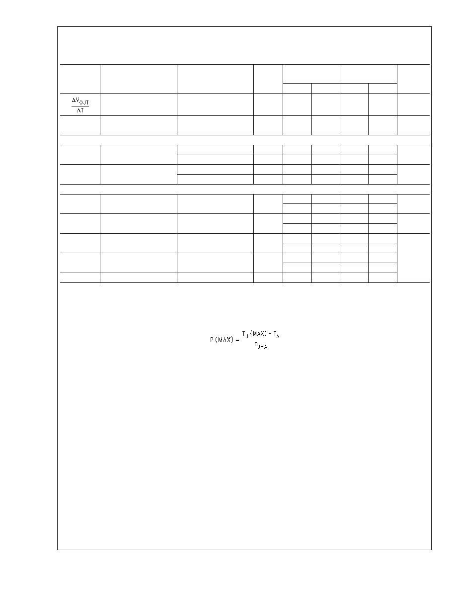
Absolute Maximum Ratings
(Note 1)
If Military/Aerospace specified devices are required,
please contact the National Semiconductor Sales Office/
Distributors for availability and specifications.
Storage Temperature Range
-65∞C to +150∞C
Operating Junction
Temperature Range
-40∞C to +125∞C
Lead Temperature
(Soldering, 5 seconds)
260∞C
ESD Rating (Note 2)
2 kV
Power Dissipation (Note 3)
Internally Limited
Input Supply Voltage
(Survival)
-0.3V to +16V
Input Supply Voltage
(Operating)
2.1V to +16V
Shutdown Pin
-0.3V to +16V
Sense Pin
-0.3V to +6V
Output Voltage
(Survival) (Note 4)
-0.3V to +16V
I
OUT
(Survival)
Short Circuit Protected
Input-Output Voltage
(Survival) (Note 5)
-0.3V to +16V
Electrical Characteristics
Limits in standard typeface are for T
J
= 25∞C, and limits in boldface type apply over the full operating temperature range. Un-
less otherwise specified: V
IN
= V
O
(NOM) + 1V, I
L
= 1 mA, C
OUT
= 4.7 µF, C
IN
= 2.2 µF, V
S/D
= 2V.
Symbol
Parameter
Conditions
Typical
LM2987/8AI-X.X
(Note 6)
LM2987/8I-X.X
(Note 6)
Units
Min
Max
Min
Max
V
O
Output Voltage
Tolerance
-0.5
0.5
-1.0
1.0
%V
NOM
0.1 mA
<
I
L
<
200 mA
-0.8
0.8
-1.6
1.6
-1.8
1.8
-2.8
2.8
Output Voltage Line
Regulation
V
O
(NOM) + 1V
V
IN
16V
0.007
0.014
0.014
%/V
0.032
0.032
V
IN
≠V
O
Dropout Voltage
(Note 7)
I
L
= 100 µA
1
2.0
2.0
mV
3.5
3.5
I
L
= 75 mA
90
120
120
170
170
I
L
= 200 mA
180
230
230
350
350
I
GND
Ground Pin Current
I
L
= 100 µA
100
120
120
µA
150
150
I
L
= 75 mA
500
800
800
1400
1400
I
L
= 200 mA
1
2.1
2.1
mA
3.7
3.7
V
S/D
<
0.3V
0.05
1.5
1.5
µA
I
O
(PK)
Peak Output Current
V
OUT
V
O
(NOM) - 5%
400
250
250
mA
I
O
(MAX)
Short Circuit Current
R
L
= 0 (Steady State)
(Note 10)
400
e
n
LP2987 Output Noise
Voltage (RMS)
BW = 300 Hz to
50 kHz, V
OUT
= 3.3V
C
OUT
= 10 µF
100
µV(RMS)
LP2988 Output Noise
Voltage (RMS)
BW = 300 Hz to 50 kHz,
V
OUT
= 3.3V
C
OUT
= 10 µF
C
BYPASS
= .01 µF
20
Ripple Rejection
f = 1 kHz, C
OUT
= 10 µF
C
BYP
= 0 (LP2988)
65
dB
LP2987/LP2988
www.national.com
9
Electrical Characteristics
(Continued)
Limits in standard typeface are for T
J
= 25∞C, and limits in boldface type apply over the full operating temperature range. Un-
less otherwise specified: V
IN
= V
O
(NOM) + 1V, I
L
= 1 mA, C
OUT
= 4.7 µF, C
IN
= 2.2 µF, V
S/D
= 2V.
Symbol
Parameter
Conditions
Typical
LM2987/8AI-X.X
(Note 6)
LM2987/8I-X.X
(Note 6)
Units
Min
Max
Min
Max
Output Voltage
Temperature Coefficient
(Note 9)
20
ppm/∞C
I
DELAY
Delay Pin Current
Source
2.2
1.6
2.8
1.6
2.8
µA
1.4
3.0
1.4
3.0
SHUTDOWN INPUT
V
S/D
S/D Input Voltage
(Note 8)
V
H
= O/P ON
1.4
1.6
1.6
V
V
L
= O/P OFF
0.55
0.18
0.18
I
S/D
S/D Input Current
V
S/D
= 0
0
-1
-1
µA
V
S/D
= 5V
5
15
15
ERROR COMPARATOR
I
OH
Output "HIGH" Leakage
V
OH
= 16V
0.01
1
1
µA
2
2
V
OL
Output "LOW" Voltage
V
IN
= V
O
(NOM) - 0.5V,
I
O
(COMP) = 300 µA
150
220
220
mV
350
350
V
THR
(MAX)
Upper Threshold Voltage
-4.6
-5.5
-3.5
-5.5
-3.5
%V
OUT
-7.7
-2.5
-7.7
-2.5
V
THR
(MIN)
Lower Threshold Voltage
-6.6
-8.9
-4.9
-8.9
-4.9
-13.0
-3.3
-13.0
-3.3
HYST
Hysteresis
2.0
Note 1: Absolute Maximum Ratings indicate limits beyond which damage to the component may occur. Electrical specifications do not apply when operating the
device outside of its rated operating conditions.
Note 2: The ESD rating of the Bypass pin is 500V (LP2988 only.)
Note 3: The maximum allowable power dissipation is a function of the maximum junction temperature, T
J
(MAX), the junction-to-ambient thermal resistance,
J-A
,
and the ambient temperature, T
A
. The maximum allowable power dissipation at any ambient temperature is calculated using:
The value of
J-A
for the SO-8 (M) package is 160∞C/W, and the mini SO-8 (MM) package is 200∞C/W. The value
J-A
for the LLP (LD) package is specifically
dependent on PCB trace area, trace material, and the number of layers and thermal vias. For improved thermal resistance and power dissipation for the LLP
package, refer to Application Note AN-1187. Exceeding the maximum allowable power dissipation will cause excessive die temperature, and the regulator will go into
thermal shutdown.
Note 4: If used in a dual-supply system where the regulator load is returned to a negative supply, the LM2987/8 output must be diode-clamped to ground.
Note 5: The output PNP structure contains a diode between the V
IN
and V
OUT
terminals that is normally reverse-biased. Forcing the output above the input will turn
on this diode and may induce a latch-up mode which can damage the part (see Application Hints).
Note 6: Limits are 100% production tested at 25∞C. Limits over the operating temperature range are guaranteed through correlation using Statistical Quality Control
(SQC) methods. The limits are used to calculate National's Average Outgoing Quality Level (AOQL).
Note 7: Dropout voltage is defined as the input to output differential at which the output voltage drops 100 mV below the value measured with a 1V differential.
Note 8: To prevent mis-operation, the Shutdown input must be driven by a signal that swings above V
H
and below V
L
with a slew rate not less than 40 mV/µs (see
Application Hints).
Note 9: Temperature coefficient is defined as the maximum (worst-case) change divided by the total temperature range.
Note 10: See Typical Performance Characteristics curves.
LP2987/LP2988
www.national.com
10
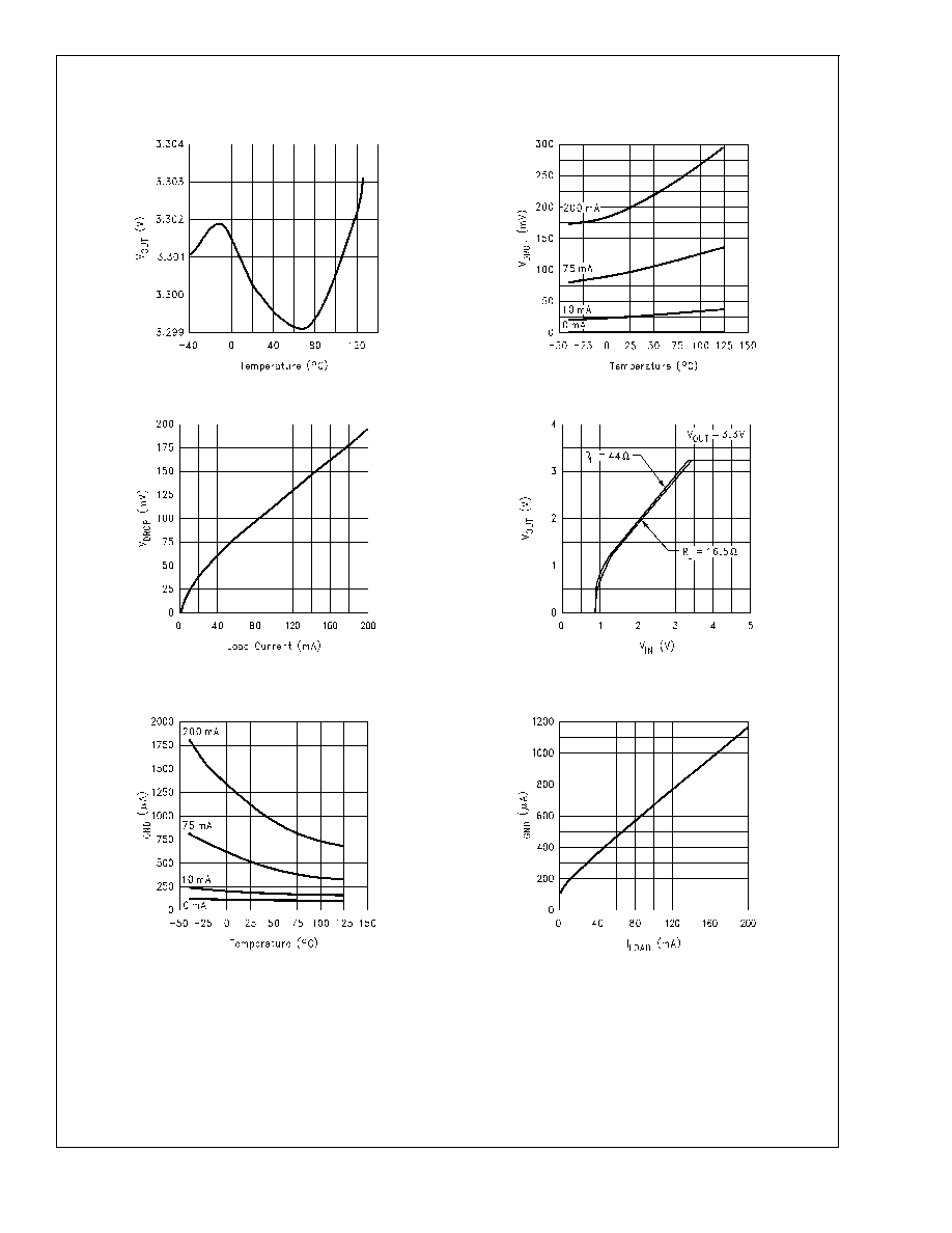
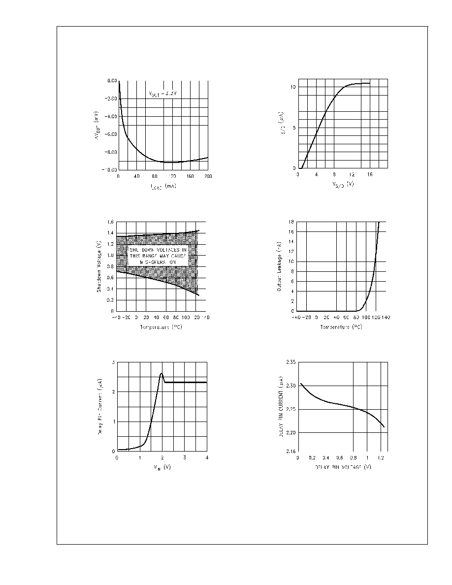
Typical Performance Characteristics
Unless otherwise specified: T
A
= 25∞C, C
OUT
= 4.7 µF,
C
IN
= 2.2 µF, S/D is tied to V
IN
, V
IN
= V
O
(NOM) + 1V, I
L
= 1 mA.
V
OUT
vs Temperature
Dropout Voltage vs Temperature
10001717
10001718
Dropout Voltage vs Load Current
Dropout Characteristics
10001719
10001720
Ground Pin Current vs
Temperature and Load
Ground Pin Current vs
Load Current
10001721
10001722
LP2987/LP2988
www.national.com
11
Typical Performance Characteristics
Unless otherwise specified: T
A
= 25∞C, C
OUT
= 4.7 µF,
C
IN
= 2.2 µF, S/D is tied to V
IN
, V
IN
= V
O
(NOM) + 1V, I
L
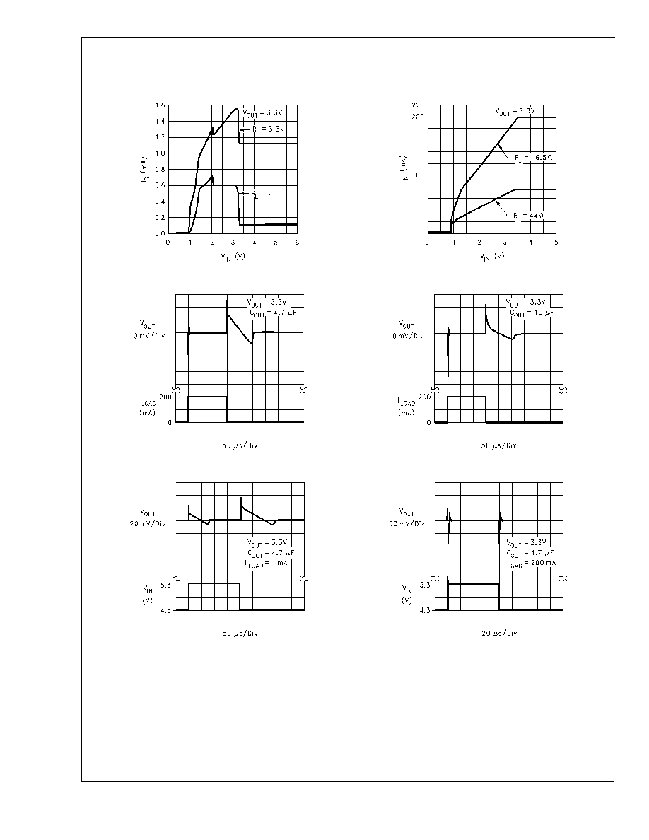
= 1 mA. (Continued)
Input Current vs V
IN
Input Current vs V
IN
10001723
10001724
Load Transient Response
Load Transient Response
10001725
10001726
Line Transient Response
Line Transient Response
10001727
10001728
LP2987/LP2988
www.national.com
12
Typical Performance Characteristics
Unless otherwise specified: T
A
= 25∞C, C
OUT
= 4.7 µF,
C
IN
= 2.2 µF, S/D is tied to V
IN
, V
IN
= V
O
(NOM) + 1V, I
L
= 1 mA. (Continued)
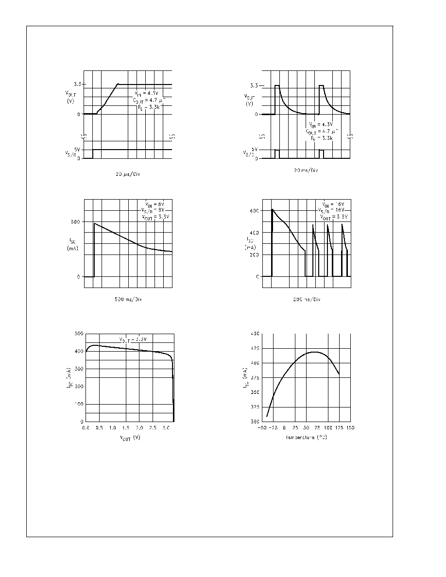
Turn-On Waveform
Turn-On Waveform
10001729
10001730
Short Circuit Current
Short Circuit Current
10001731
10001732
Short Circuit Current
vs Output Voltage
Instantaneous Short Circuit Current
vs Temperature
10001733
10001734
LP2987/LP2988
www.national.com
13
Typical Performance Characteristics
Unless otherwise specified: T
A
= 25∞C, C
OUT
= 4.7 µF,
C
IN
= 2.2 µF, S/D is tied to V
IN
, V
IN
= V
O
(NOM) + 1V, I
L
= 1 mA. (Continued)
DC Load Regulation
Shutdown Pin Current vs
Shutdown Pin Voltage
10001735
10001736
Shutdown Voltage
vs Temperature
Input to Output Leakage
vs Temperature
10001737
10001738
Delay Pin Current vs V
IN
Delay Pin Current vs
Delay Pin Voltage
10001745
10001748
LP2987/LP2988
www.national.com
14
Typical Performance Characteristics
Unless otherwise specified: T
A
= 25∞C, C
OUT
= 4.7 µF,
C
IN
= 2.2 µF, S/D is tied to V
IN
, V
IN
= V
O
(NOM) + 1V, I
L
= 1 mA. (Continued)
Delay Sink Current
vs Temperature
Delay Sink Current vs Temperature
10001747
10001746
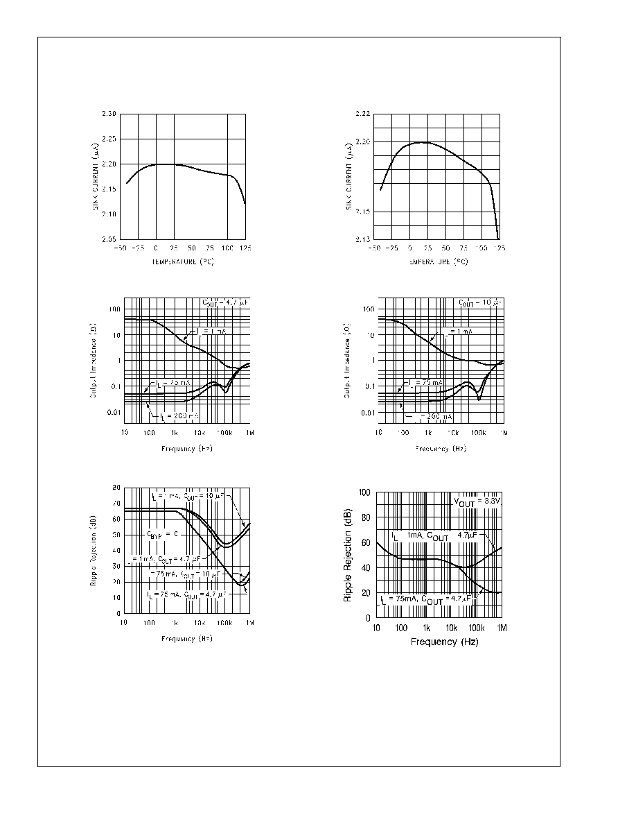
Output Impedance vs Frequency
Output Impedance vs Frequency
10001740
10001741
Ripple Rejection (LP2987)
Ripple Rejection (LP2988)
10001742
10001751
LP2987/LP2988
www.national.com
15
Typical Performance Characteristics
Unless otherwise specified: T
A
= 25∞C, C
OUT
= 4.7 µF,
C
IN
= 2.2 µF, S/D is tied to V
IN
, V
IN
= V
O
(NOM) + 1V, I
L
= 1 mA. (Continued)
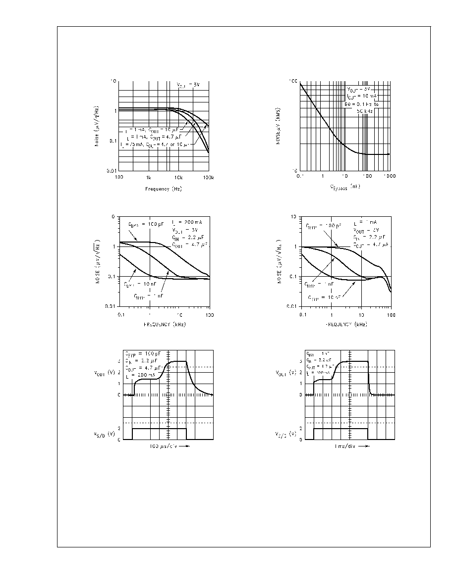
Output Noise Density (LP2987)
Output Noise Voltage (LP2988)
10001739
10001744
Output Noise Density (LP2988)
Output Noise Density (LP2988)
10001752
10001753
Turn-On Time (LP2988)
Turn-On Time (LP2988)
10001754
10001755
LP2987/LP2988
www.national.com
16
Typical Performance Characteristics
Unless otherwise specified: T
A
= 25∞C, C
OUT
= 4.7 µF,
C
IN
= 2.2 µF, S/D is tied to V
IN
, V
IN
= V
O
(NOM) + 1V, I
L
= 1 mA. (Continued)
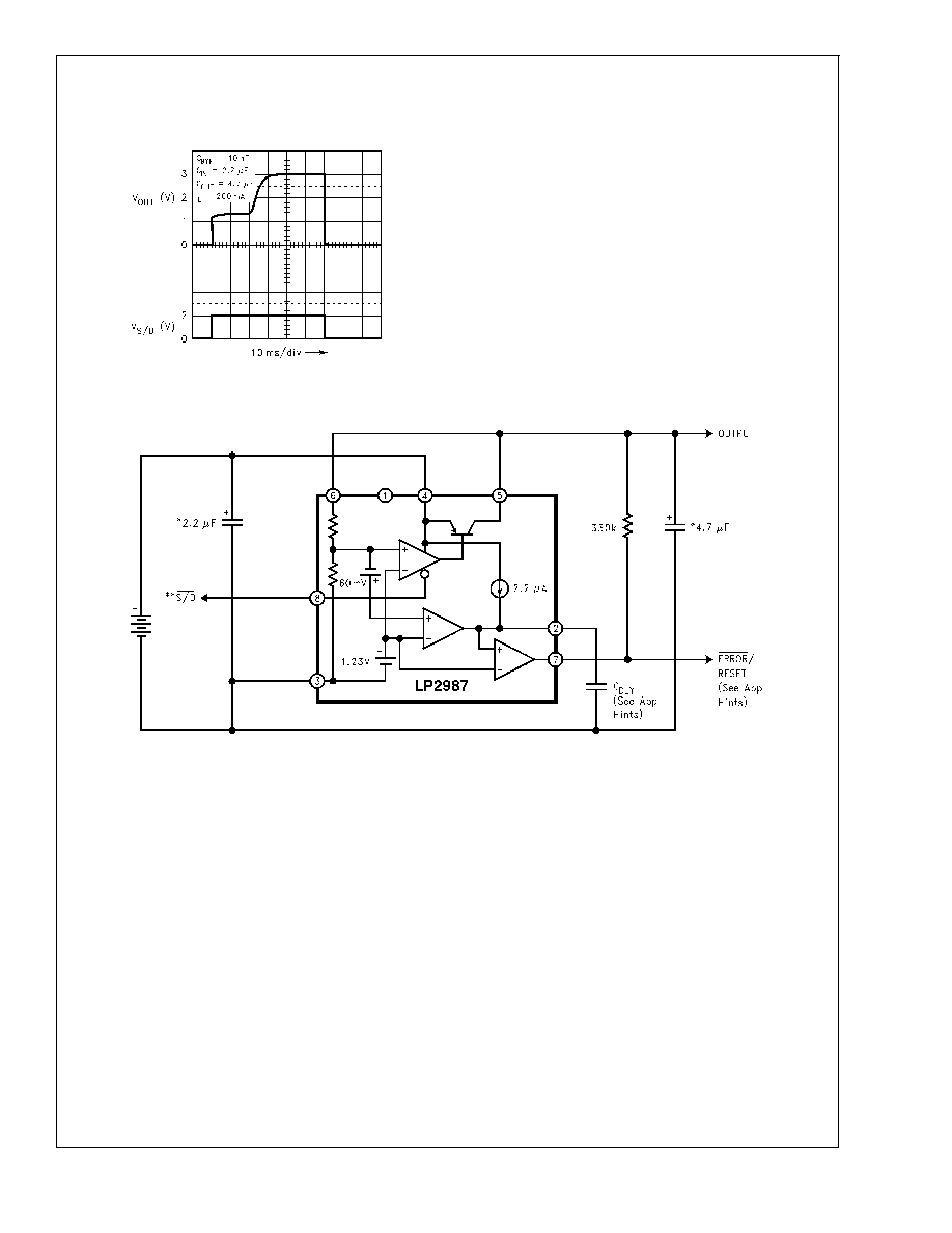
Turn-On Time (LP2988)
10001756
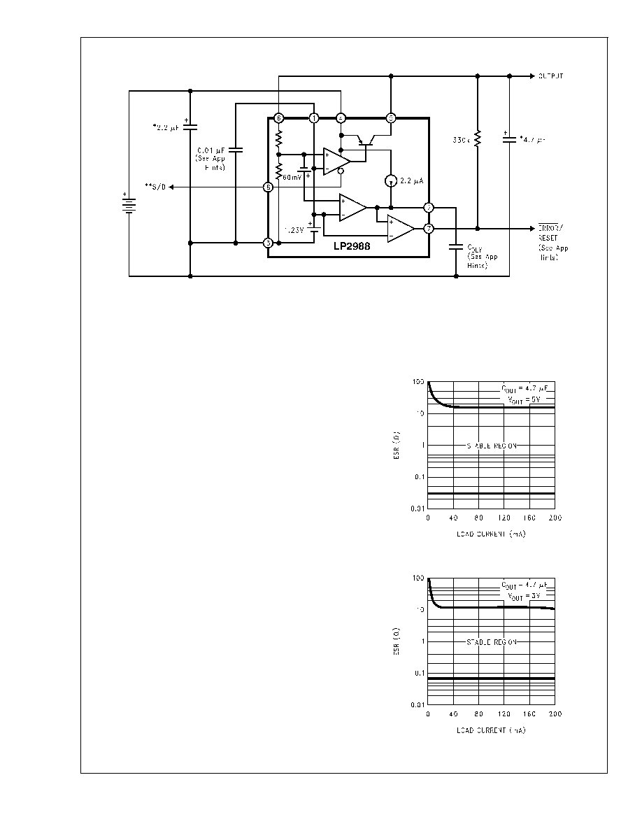
Basic Application Circuits
10001705
LP2987/LP2988
www.national.com
17
Basic Application Circuits
(Continued)
10001706
*Capacitance value shown is minimum required to assure stability, but may be increased without limit. Larger output capacitor provides improved dynamic
response.
**Shutdown must be actively terminated (see Application Hints). Tie to INPUT (pin 4) if not used.
Application Hints
LLP Package Devices
The LP2987/LP2988 is offered in the 8 lead LLP surface
mount package to allow for increased power dissipation
compared to the SO-8 and Mini SO-8. For details on thermal
performance as well as mounting and soldering specifica-
tions, refer to Application Note AN-1187.
EXTERNAL CAPACITORS
As with any low-dropout regulator, external capacitors are
required to assure stability. These capacitors must be cor-
rectly selected for proper performance.
INPUT CAPACITOR: An input capacitor (
2.2 µF) is re-
quired between the LP2987/8 input and ground (amount of
capacitance may be increased without limit).
This capacitor must be located a distance of not more than
0.5" from the input pin and returned to a clean analog
ground. Any good quality ceramic or tantalum may be used
for this capacitor.
OUTPUT CAPACITOR: The output capacitor must meet the
requirement for minimum amount of capacitance and also
have an appropriate E.S.R. (equivalent series resistance)
value.
Curves are provided which show the allowable ESR range
as a function of load current for 3V and 5V outputs.
ESR Curves For 5V Output
10001707
ESR Curves For 3V Output
10001708
LP2987/LP2988
www.national.com
18
Application Hints
(Continued)
IMPORTANT: The output capacitor must maintain its ESR in
the stable region
over the full operating temperature range of
the application to assure stability.
The minimum required amount of output capacitance is
4.7 µF. Output capacitor size can be increased without limit.
It is important to remember that capacitor tolerance and
variation with temperature must be taken into consideration
when selecting an output capacitor so that the minimum
required amount of output capacitance is provided over the
full operating temperature range. A good Tantalum capacitor
will show very little variation with temperature, but a ceramic
may not be as good (see next section).
The output capacitor should be located not more than 0.5"
from the output pin and returned to a clean analog ground.
CAPACITOR CHARACTERISTICS
TANTALUM: A solid tantalum capacitor is the best choice for
the output capacitor on the LM2987/8. Available from many
sources, their typical ESR is very close to the ideal value
required on the output of many LDO regulators.
Tantalums also have good temperature stability: a 4.7 µF
was tested and showed only a 10% decline in capacitance
as the temperature was decreased from +125∞C to -40∞C.
The ESR increased only about 2:1 over the same range of
temperature.
However, it should be noted that the increasing ESR at lower
temperatures present in all tantalums can cause oscillations
when marginal quality capacitors are used (where the ESR
of the capacitor is near the upper limit of the stability range at
room temperature).
CERAMIC: The ESR of ceramic capacitor can be low
enough to cause an LDO regulator to oscillate: a 2.2 µF
ceramic was measured and found to have an ESR of 15 m
.
If a ceramic capacitor is to be used on the LP2987/8 output,
a 1
resistor should be placed in series with the capacitor to
provide a minimum ESR for the regulator.
A disadvantage of ceramic capacitors is that their capaci-
tance varies a lot with temperature: Large ceramic capaci-
tors are typically manufactured with the Z5U temperature
characteristic, which results in the capacitance dropping by
50% as the temperature goes from 25∞C to 80∞C.
This means you have to buy a capacitor with twice the
minimum C
OUT
to assure stable operation up to 80∞C.
ALUMINUM: The large physical size of aluminum electrolyt-
ics makes them unsuitable for most applications. Their ESR
characteristics are also not well suited to the requirements of
LDO regulators. The ESR of a typical aluminum electrolytic
is higher than a tantalum, and it also varies greatly with
temperature.
A typical aluminum electrolytic can exhibit an ESR increase
of 50X when going from 20∞C to -40∞C. Also, some alumi-
num electrolytics can not be used below -25∞C because the
electrolyte will freeze.
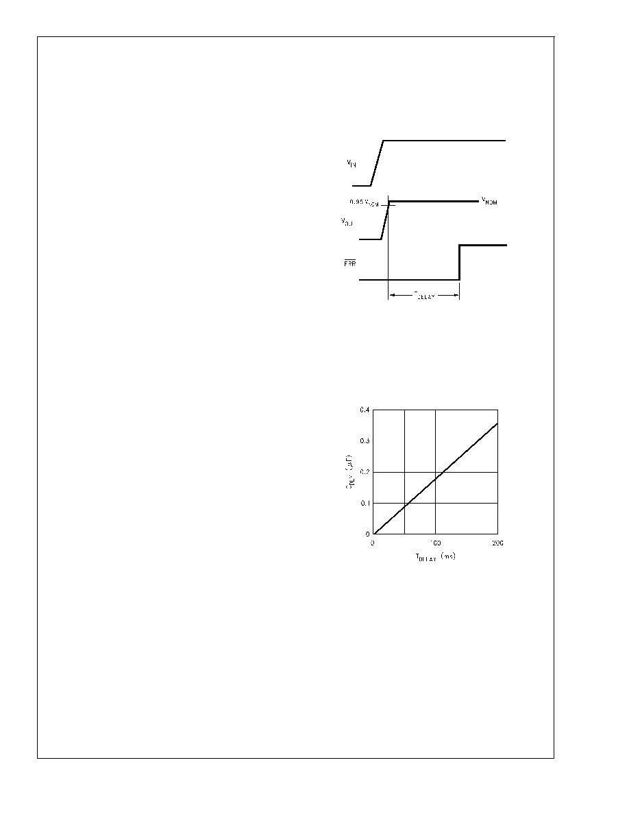
POWER-ON RESET DELAY
A power-on reset function can be easily implemented using
the LP2987/8 by adding a single external capacitor to the
Delay pin. The Error output provides the power-on reset
signal when input power is applied to the regulator.
The reset signal stays low for a pre-set time period after
power is applied to the regulator, and then goes high (see
Timing Diagram below).
10001709
Timing Diagram for Power-Up
The external capacitor c
DLY
sets the delay time (T
DELAY
).
The value of capacitor required for a given time delay may
be calculated using the formula:
C
DLY
= T
DELAY
/(5.59 X 10
5
)
To simplify design, a plot is provided below which shows
values of C
DLY
versus delay time.
10001711
Plot of C
DLY
vs T
DELAY
LP2987/LP2988
www.national.com
19
Application Hints
(Continued)
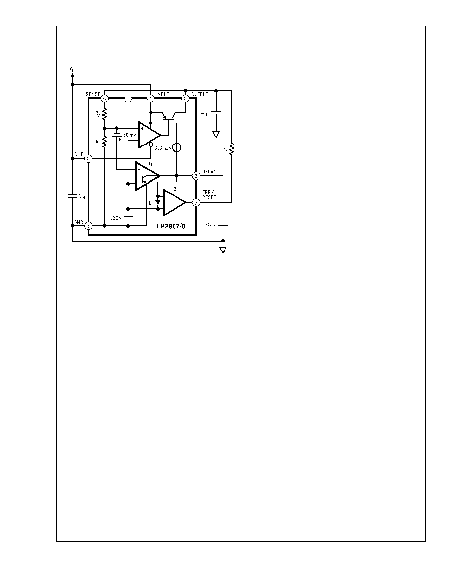
DETAILS OF ERR/RESET CIRCUIT OPERATION: (Refer
to LP2987/8 Equivalent Circuit).
10001710
LP2987/8 Equivalent Circuit
The output of comparator U2 is the ERR/RESET flag. Since
it is an open-collector output, it requires the use of a pull-up
resistor (R
P
). The 1.23V reference is tied to the inverting
input of U2, which means that its output is controlled by the
voltage applied to the non-inverting input.
The output of U1 (also an open-collector) will force the
non-inverting input of U2 to go low whenever the LP2987/8
regulated output drops about 5% below nominal.
U1's inverting input is also held at 1.23V. The other input
samples the regulated output through a resistive divider (R
A
and R
B
). When the regulated output is at nominal voltage,
the voltage at the divider tap point will be 1.23V. If this
voltage drops about 60 mV below 1.23V, the output of U1 will
go low forcing the output of U2 low (which is the ERROR
state).
Power-ON reset delay occurs when a capacitor (shown as
C
DLY
) is connected to the Delay pin. At turn-ON, this capaci-
tor is initially fully discharged (which means the voltage at
the Delay pin is 0V). The output of U1 keeps C
DLY
fully
discharged (by sinking the 2.2 µA from the current source)
until the regulator output voltage comes up to within about
5% of nominal. At this point, U1's output stops sinking cur-
rent and the 2.2 µA starts charging up C
DLY
.
When the voltage across C
DLY
reaches 1.23V, the output of
U2 will go high (note that D1 limits the maximum voltage to
about 2V).
SELECTING C
DLY
: The maximum recommended value for
this capacitor is 1 µF. The capacitor must not have exces-
sively high leakage current, since it is being charged from a
2.2 µA current source.
Aluminum electrolytics can not be used, but good-quality
tantalum, ceremic, mica, or film types will work.
SHUTDOWN INPUT OPERATION
The LP2987/8 is shut off by driving the Shutdown input low,
and turned on by pulling it high. If this feature is not to be
used, the Shutdown input should be tied to V
IN
to keep the
regulator output on at all times.
To assure proper operation, the signal source used to drive
the Shutdown input must be able to swing above and below
the specified turn-on/turn-off voltage thresholds listed as V
H
and V
L
, respectively (see Electrical Characteristics).
It is also important that the turn-on (and turn-off) voltage
signals applied to the Shutdown input have a slew rate which
is not less than 40 mV/µs.
CAUTION: the regulator output state can not be guaranteed
if a slow-moving AC (or DC) signal is applied that is in the
range between V
H
and V
L
.
REVERSE INPUT-OUTPUT VOLTAGE
The PNP power transistor used as the pass element in the
LP2987/8 has an inherent diode connected between the
regulator output and input.
During normal operation (where the input voltage is higher
than the output) this diode is reverse-biased.
However, if the output is pulled above the input, this diode
will turn ON and current will flow into the regulator output.
In such cases, a parasitic SCR can latch which will allow a
high current to flow into V
IN
(and out the ground pin), which
can damage the part.
In any application where the output may be pulled above the
input, an external Schottky diode must be connected from
V
IN
to V
OUT
(cathode on V
IN
, anode on V
OUT
), to limit the
reverse voltage across the LP2987/8 to 0.3V (see Absolute
Maximum Ratings).
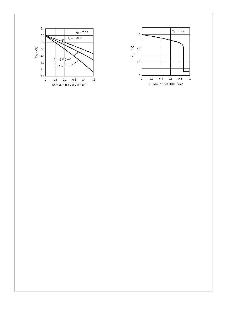
BYPASS CAPACITOR (LP2988)
The capacitor connected to the Bypass pin must have very
low leakage. The current flowing out of the Bypass pin
comes from the Bandgap reference, which is used to set the
output voltage. Since the Bandgap circuit has only a few
microamps flowing in it, loading effects due to leakage cur-
rent will cause a change in the regulated output voltage.
Curves are provided which show the effect of loading the
Bypass pin on the regulated output voltage.
Care must be taken to ensure that the capacitor selected for
bypass will not have significant leakage current over the
operating temperature range of the application.
A high quality ceramic capacitor which uses either NPO or
COG type dielectiric material will typically have very low
leakage. Small surface-mount polypropolene or polycarbon-
ate film capacitors also have extremely low leakage, but are
slightly larger in size than ceramics.
LP2987/LP2988
www.national.com
20
Application Hints
(Continued)
10001749
10001750
LP2987/LP2988
www.national.com
21
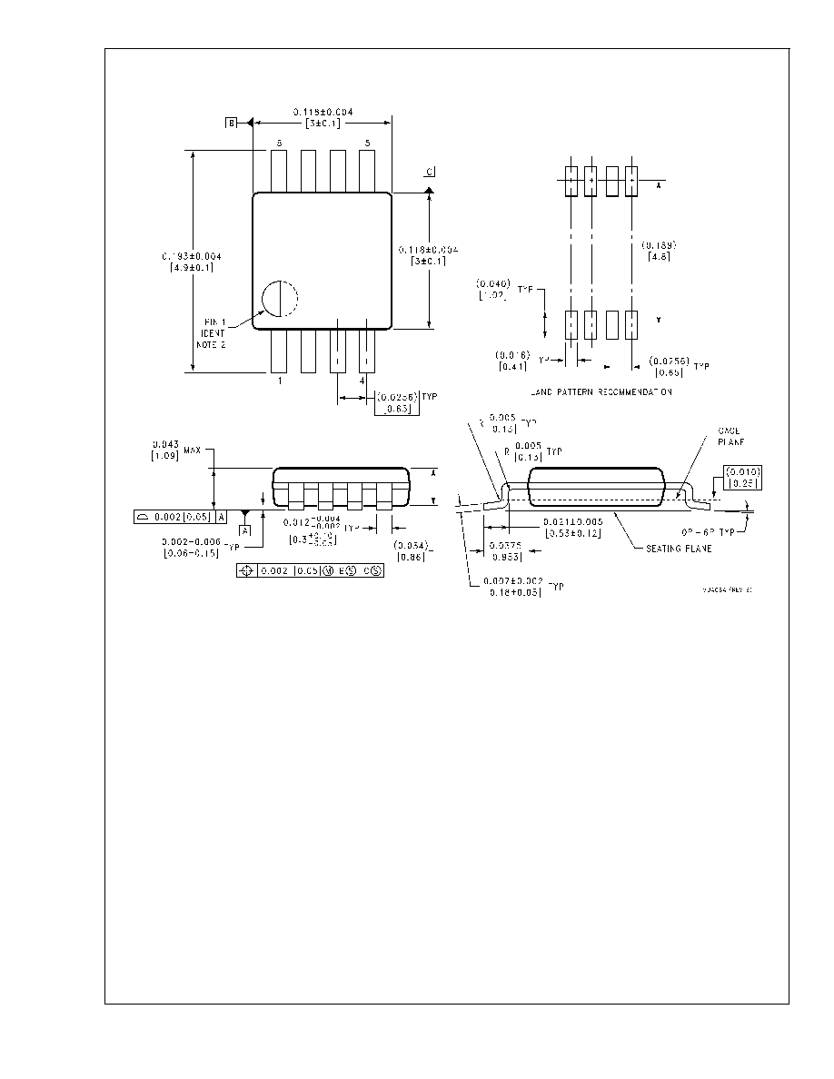
Physical Dimensions
inches (millimeters)
unless otherwise noted
Mini SO-8 Package Type MM
NS Package Number MUA08A
LP2987/LP2988
www.national.com
22
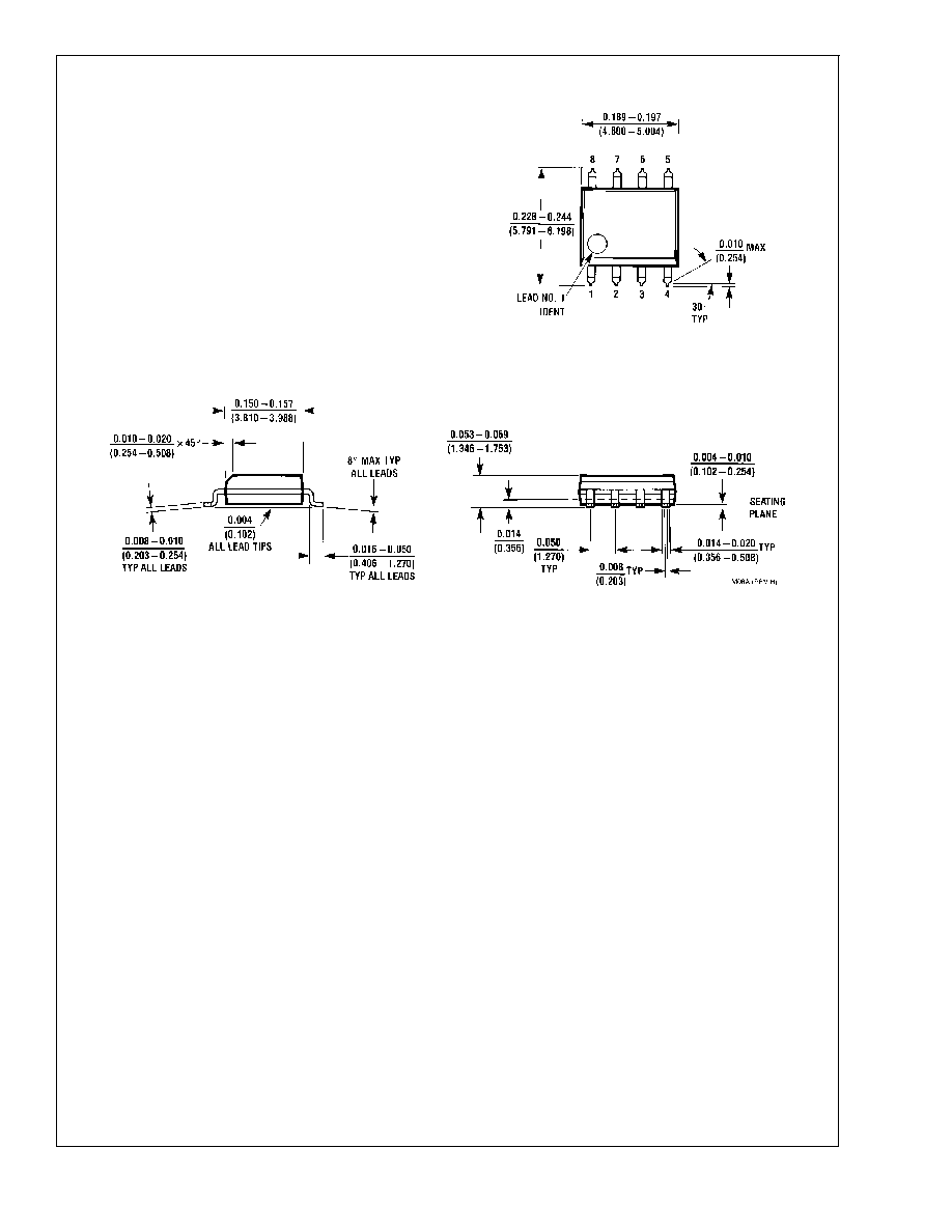
Physical Dimensions
inches (millimeters) unless otherwise noted (Continued)
SO-8 Package Type M
NS Package Number M08A
LP2987/LP2988
www.national.com
23

Physical Dimensions
inches (millimeters) unless otherwise noted (Continued)
8-Lead LLP Surface Mount Package
NS Package Number LDC08A
LIFE SUPPORT POLICY
NATIONAL'S PRODUCTS ARE NOT AUTHORIZED FOR USE AS CRITICAL COMPONENTS IN LIFE SUPPORT
DEVICES OR SYSTEMS WITHOUT THE EXPRESS WRITTEN APPROVAL OF THE PRESIDENT AND GENERAL
COUNSEL OF NATIONAL SEMICONDUCTOR CORPORATION. As used herein:
1. Life support devices or systems are devices or
systems which, (a) are intended for surgical implant
into the body, or (b) support or sustain life, and
whose failure to perform when properly used in
accordance with instructions for use provided in the
labeling, can be reasonably expected to result in a
significant injury to the user.
2. A critical component is any component of a life
support device or system whose failure to perform
can be reasonably expected to cause the failure of
the life support device or system, or to affect its
safety or effectiveness.
National Semiconductor
Corporation
Americas
Email: support@nsc.com
National Semiconductor
Europe
Fax: +49 (0) 180-530 85 86
Email: europe.support@nsc.com
Deutsch Tel: +49 (0) 69 9508 6208
English
Tel: +44 (0) 870 24 0 2171
FranÁais Tel: +33 (0) 1 41 91 8790
National Semiconductor
Asia Pacific Customer
Response Group
Tel: 65-2544466
Fax: 65-2504466
Email: ap.support@nsc.com
National Semiconductor
Japan Ltd.
Tel: 81-3-5639-7560
Fax: 81-3-5639-7507
www.national.com
LP2987/LP2988
Micropower
,
200
mA
Ultra
Low-Dropout
V
oltage
Regulator
with
Programmable
Power-On
Reset
Delay
National does not assume any responsibility for use of any circuitry described, no circuit patent licenses are implied and National reserves the right at any time without notice to change said circuitry and specifications.