
LP2989
Micropower/Low Noise, 500 mA Ultra Low-Dropout
Regulator
For Use with Ceramic Output Capacitors
General Description
The LP2989 is a fixed-output 500 mA precision LDO regu-
lator designed for use with ceramic output capacitors.
Output noise can be reduced to 18µV (typical) by connecting
an external 10 nF capacitor to the bypass pin.
Using an optimized VIP
TM
(Vertically Integrated PNP) pro-
cess, the LP2989 delivers superior performance:
Dropout Voltage: Typically 310 mV
@
500 mA load, and 1
mV
@
100 µA load.
Ground Pin Current: Typically 3 mA
@
500 mA load, and
110 µA
@
100 µA load.
Sleep Mode: The LP2989 draws less than 0.8 µA quiescent
current when shutdown pin is pulled low.
Error Flag: The built-in error flag goes low when the output
drops approximately 5% below nominal.
Precision Output: Guaranteed output voltage accuracy is
0.75% ("A" grade) and 1.25% (standard grade) at room
temperature.
For output voltages
<
2V, see LP2989LV datasheet.
Features
n
Ultra low dropout voltage
n
Guaranteed 500 mA continuous output current
n
Very low output noise with external capacitor
n
SO-8, Mini SO-8, 8 Lead LLP surface mount packages
n
<
0.8 µA quiescent current when shutdown
n
Low ground pin current at all loads
n
0.75% output voltage accuracy ("A" grade)
n
High peak current capability (800 mA typical)
n
Wide supply voltage range (16V max)
n
Overtemperature/overcurrent protection
n
-40∞C to +125∞C junction temperature range
Applications
n
Notebook/Desktop PC
n
PDA/Palmtop Computer
n
Wireless Communication Terminals
n
SMPS Post-Regulator
Block Diagram
10133901
VIP
TM
is a trademark of National Semiconductor Corporation.
June 2002
LP2989
Micropower/Low
Noise,
500
mA
Ultra
Low-Dropout
Regulator
For
Use
with
Ceramic
Output
Capacitors
© 2002 National Semiconductor Corporation
DS101339
www.national.com
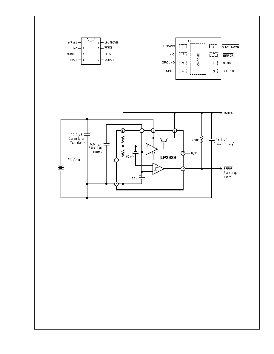
Connection Diagrams
Surface Mount Packages:
8 Lead LLP Surface Mount Package
10133902
SO-8/Mini SO-8 Package
See NS Package Drawing Numbers M08A/MUA08A
10133950
Top View
See NS Package Number LDC08A
Basic Application Circuit
10133903
*Capacitance values shown are minimum required to assure stability, but may be increased without limit. Larger output capacitor provides improved dynamic
response. See Application Hints.
**Shutdown must be actively terminated (see App. Hints). Tie to INPUT (Pin4) if not used
LP2989
www.national.com
2
Ordering Information
TABLE 1. Package Marking and Ordering Information
Output Voltage
Grade
Order Information
Package Marking
Supplied as:
8 Lead LLP
2.5
A
LP2989AILD-2.5
L01FA
1000 Units on Tape and Reel
2.5
A
LP2989AILDX-2.5
L01FA
4500 Units on Tape and Reel
2.5
STD
LP2989ILD-2.5
L01FAB
1000 Units on Tape and Reel
2.5
STD
LP2989ILDX-2.5
L01FAB
4500 Units on Tape and Reel
2.8
A
LP2989AILD-2.8
L000A
1000 Units on Tape and Reel
2.8
A
LP2989AILDX-2.8
L000A
4500 Units on Tape and Reel
2.8
STD
LP2989ILD-2.8
L000AB
1000 Units on Tape and Reel
2.8
STD
LP2989ILDX-2.8
L000AB
4500 Units on Tape and Reel
2.85
A
LP2989AILD-285
L01TA
1000 Units on Tape and Reel
2.85
A
LP2989AILDX-285
L01TA
4500 Units on Tape and Reel
2.85
STD
LP2989ILD-285
L01TAB
1000 Units on Tape and Reel
2.85
STD
LP2989ILDX-285
L01TAB
4500 Units on Tape and Reel
3.0
A
LP2989AILD-3.0
L01HA
1000 Units on Tape and Reel
3.0
A
LP2989AILDX-3.0
L01HA
4500 Units on Tape and Reel
3.0
STD
LP2989ILD-3.0
L01HAB
1000 Units on Tape and Reel
3.0
STD
LP2989ILDX-3.0
L01HAB
4500 Units on Tape and Reel
3.3
A
LP2989AILD-3.3
L01JA
1000 Units on Tape and Reel
3.3
A
LP2989AILDX-3.3
L01JA
4500 Units on Tape and Reel
3.3
STD
LP2989ILD-3.3
L01JAB
1000 Units on Tape and Reel
3.3
STD
LP2989ILDX-3.3
L01JAB
4500 Units on Tape and Reel
3.6
A
LP2989AILD-3.6
L019A
1000 Units on Tape and Reel
3.6
A
LP2989AILDX-3.6
L019A
4500 Units on Tape and Reel
3.6
STD
LP2989ILD-3.6
L019AB
1000 Units on Tape and Reel
3.6
STD
LP2989ILDX-3.6
L019AB
4500 Units on Tape and Reel
4.0
A
LP2989AILD-4.0
L01LA
1000 Units on Tape and Reel
4.0
A
LP2989AILDX-4.0
L01LA
4500 Units on Tape and Reel
4.0
STD
LP2989ILD-4.0
L01LAB
1000 Units on Tape and Reel
4.0
STD
LP2989ILDX-4.0
L01LAB
4500 Units on Tape and Reel
5.0
A
LP2989AILD-5.0
L01KA
1000 Units on Tape and Reel
5.0
A
LP2989AILDX-5.0
L01KA
4500 Units on Tape and Reel
5.0
STD
LP2989ILD-5.0
L01KAB
1000 Units on Tape and Reel
5.0
STD
LP2989ILDX-5.0
L01KAB
4500 Units on Tape and Reel
8 Lead MSOP (MM)
2.5
A
LP2989AIMM-2.5
LA0A
1000 Units on Tape and Reel
2.5
A
LP2989AIMMX-2.5
LA0A
3500 Units on Tape and Reel
2.5
STD
LP2989IMM-2.5
LA0B
1000 Units on Tape and Reel
2.5
STD
LP2989IMMX-2.5
LA0B
3500 Units on Tape and Reel
2.8
A
LP2989AIMM-2.8
LA6A
1000 Units on Tape and Reel
2.8
A
LP2989AIMMX-2.8
LA6A
3500 Units on Tape and Reel
2.8
STD
LP2989IMM-2.8
LA6B
1000 Units on Tape and Reel
2.8
STD
LP2989IMMX-2.8
LA6B
3500 Units on Tape and Reel
3.0
A
LP2989AIMM-3.0
LA1A
1000 Units on Tape and Reel
3.0
A
LP2989AIMMX-3.0
LA1A
3500 Units on Tape and Reel
3.0
STD
LP2989IMM-3.0
LA1B
1000 Units on Tape and Reel
3.0
STD
LP2989IMMX-3.0
LA1B
3500 Units on Tape and Reel
3.3
A
LP2989AIMM-3.3
LA2A
1000 Units on Tape and Reel
3.3
A
LP2989AIMMX-3.3
LA2A
3500 Units on Tape and Reel
LP2989
www.national.com
3
Ordering Information
(Continued)
TABLE 1. Package Marking and Ordering Information (Continued)
Output Voltage
Grade
Order Information
Package Marking
Supplied as:
3.3
STD
LP2989IMM-3.3
LA2B
1000 Units on Tape and Reel
3.3
STD
LP2989IMMX-3.3
LA2B
3500 Units on Tape and Reel
5.0
A
LP2989AIMM-5.0
LA4A
1000 Units on Tape and Reel
5.0
A
LP2989AIMMX-5.0
LA4A
3500 Units on Tape and Reel
5.0
STD
LP2989IMM-5.0
LA4B
1000 Units on Tape and Reel
5.0
STD
LP2989IMMX-5.0
LA4B
3500 Units on Tape and Reel
LP2989
www.national.com
4
Ordering Information
(Continued)
TABLE 1. Package Marking and Ordering Information (Continued)
Output Voltage
Grade
Order Information
Package Marking
Supplied as:
SO-8 (M)
2.5
A
LP2989AIMX-2.5
LP2989AIM2.5
2500 Units on Tape and Reel
2.5
A
LP2989AIM-2.5
LP2989AIM2.5
Shipped in Anti-Static Rails
2.5
STD
LP2989IMX-2.5
LP2989IM2.5
2500 Units on Tape and Reel
2.5
STD
LP2989IM-2.5
LP2989IM2.5
Shipped in Anti-Static Rails
3.3
A
LP2989AIMX-3.3
LP2989AIM3.3
2500 Units on Tape and Reel
3.3
A
LP2989AIM-3.3
LP2989AIM3.3
Shipped in Anti-Static Rails
3.3
STD
LP2989IMX-3.3
LP2989IM3.3
2500 Units on Tape and Reel
3.3
STD
LP2989IM-3.3
LP2989IM3.3
Shipped in Anti-Static Rails
5.0
A
LP2989AIMX-5.0
LP2989AIM5.0
2500 Units on Tape and Reel
5.0
A
LP2989AIM-5.0
LP2989AIM5.0
Shipped in Anti-Static Rails
5.0
STD
LP2989IMX-5.0
LP2989IM5.0
2500 Units on Tape and Reel
5.0
STD
LP2989IM-5.0
LP2989IM5.0
Shipped in Anti-Static Rails
For output voltages
<
2V, see LP2989LV datasheet.
LP2989
www.national.com
5
Absolute Maximum Ratings
(Note 1)
If Military/Aerospace specified devices are required,
please contact the National Semiconductor Sales Office/
Distributors for availability and specifications.
Storage Temperature Range
-65∞C to +150∞C
Operating Junction
Temperature
Range
-40∞C to +125∞C
Lead Temperature
(Soldering, 5
seconds)
260∞C
ESD Rating (Note 2)
2 kV
Power Dissipation (Note 3)
Internally Limited
Input Supply Voltage
(Survival)
-0.3V to +16V
Input Supply Voltage
(Operating)
2.1V to +16V
Sense Pin
-0.3V to +6V
Output Voltage
(Survival)
(Note 4)
-0.3V to +16V
I
OUT
(Survival)
Short Circuit
Protected
Input-Output Voltage
(Survival)
(Note 5)
-0.3V to +16V
Electrical Characteristics
Limits in standard typeface are for T
J
= 25∞C, and limits in boldface type apply over the full operating temperature range. Un-
less otherwise specified: V
IN
= V
O
(NOM) + 1V, I
L
= 1 mA, C
OUT
= 4.7 µF, C
IN
= 2.2 µF, V
S/D
= 2V.
Symbol
Parameter
Conditions
Typical
LP2989AI-X.X
(Note 6)
LP2989I-X.X
(Note 6)
Units
Min
Max
Min
Max
V
O
Output Voltage
Tolerance
-0.75
0.75
-1.25
1.25
%V
NOM
1 mA
<
I
L
<
500 mA
V
O
(NOM) + 1V
V
IN
16V
-1.5
1.5
-2.5
2.5
-4.0
2.5
-5.0
3.5
1 mA
<
I
L
<
500 mA
V
O
(NOM) + 1V
V
IN
16V
-25∞C
T
J
125∞C
-3.5
2.5
-4.5
3.5
Output Voltage Line
Regulation
V
O
(NOM) + 1V
V
IN
16V
0.005
0.014
0.014
%/V
0.032
0.032
Load Regulation
1 mA
<
I
L
<
500 mA
0.4
%V
NOM
V
IN
≠V
O
Dropout Voltage
(Note 7)
I
L
= 100 µA
1
3
3
mV
4
4
I
L
= 200 mA
150
200
200
300
300
I
L
= 500 mA
310
425
425
650
650
I
GND
Ground Pin Current
I
L
= 100 µA
110
175
175
µA
200
200
I
L
= 200 mA
1
2
2
mA
3.5
3.5
I
L
= 500 mA
3
6
6
9
9
V
S/D
<
0.18V
0.5
2
2
µA
V
S/D
<
0.4V
0.05
0.8
0.8
I
O
(PK)
Peak Output Current
V
OUT
V
O
(NOM) - 5%
800
600
600
mA
I
O
(MAX)
Short Circuit Current
R
L
= 0 (Steady State)
(Note 9)
1000
e
n
Output Noise Voltage
(RMS)
BW = 100 Hz to
100 kHz, C
OUT
= 10 µF
C
BYPASS
= .01 µF
V
OUT
= 2.5V
18
µV(RMS)
LP2989
www.national.com
6

Electrical Characteristics
(Continued)
Limits in standard typeface are for T
J
= 25∞C, and limits in boldface type apply over the full operating temperature range. Un-
less otherwise specified: V
IN
= V
O
(NOM) + 1V, I
L
= 1 mA, C
OUT
= 4.7 µF, C
IN
= 2.2 µF, V
S/D
= 2V.
Symbol
Parameter
Conditions
Typical
LP2989AI-X.X
(Note 6)
LP2989I-X.X
(Note 6)
Units
Min
Max
Min
Max
Ripple Rejection
f = 1 kHz, C
OUT
= 10 µF
60
dB
Output Voltage
Temperature Coefficient
(Note 8)
20
ppm/∞C
SHUTDOWN INPUT
V
S/D
S/D Input Voltage
V
H
= O/P ON
1.4
1.6
1.6
V
V
L
= O/P OFF
I
IN
2 µA
0.50
0.18
0.18
I
S/D
S/D Input Current
V
S/D
= 0
0.001
-1
-1
µA
V
S/D
= 5V
5
15
15
ERROR COMPARATOR
I
OH
Output "HIGH" Leakage
V
OH
= 16V
0.001
1
1
µA
2
2
V
OL
Output "LOW" Voltage
V
IN
= V
O
(NOM) - 0.5V,
I
O
(COMP) = 150 µA
150
220
220
mV
350
350
V
THR
(MAX)
Upper Threshold Voltage
-4.8
-6.0
-3.5
-6.0
-3.5
%V
OUT
-8.3
-2.5
-8.3
-2.5
V
THR
(MIN)
Lower Threshold Voltage
-6.6
-8.9
-4.9
-8.9
-4.9
-13.0
-3.0
-13.0
-3.0
HYST
Hysteresis
2.0
Note 1: Absolute Maximum Ratings indicate limits beyond which damage to the component may occur. Electrical specifications do not apply when operating the
device outside of its rated operating conditions.
Note 2: ESD testing was performed using Human Body Model, a 100 pF capacitor discharged through a 1.5 k
resistor.
Note 3: The maximum allowable power dissipation is a function of the maximum junction temperature, T
J
(MAX), the junction-to-ambient thermal resistance,
J-A
,
and the ambient temperature, T
A
. The maximum allowable power dissipation at any ambient temperature is calculated using:
The value of
J-A
for the SO-8 (M) package is 160∞C/W and the mini SO-8 (MM) package is 200∞C/W. The value
J-A
for the LLP (LD) package is specifically
dependent on PCB trace area, trace material, and the number of layers and thermal vias. For improved thermal resistance and power dissipation for the LLP
package, refer to Application Note AN-1187. Exceeding the maximum allowable power dissipation will cause excessive die temperature, and the regulator will go into
thermal shutdown.
Note 4: If used in a dual-supply system where the regulator load is returned to a negative supply, the LP2989 output must be diode-clamped to ground.
Note 5: The output PNP structure contains a diode between the V
IN
and V
OUT
terminals that is normally reverse-biased. Forcing the output above the input will turn
on this diode and may induce a latch-up mode which can damage the part (see Application Hints).
Note 6: Limits are 100% production tested at 25∞C. Limits over the operating temperature range are guaranteed through correlation using Statistical Quality Control
(SQC) methods. The limits are used to calculate National's Average Outgoing Quality Level (AOQL).
Note 7: Dropout voltage is defined as the input to output differential at which the output voltage drops 100 mV below the value measured with a 1V differential.
Note 8: Temperature coefficient is defined as the maximum (worst-case) change divided by the total temperature range.
Note 9: See Typical Performance Characteristics curves.
LP2989
www.national.com
7
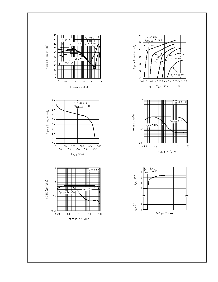
Typical Performance Characteristics
Unless otherwise specified: T
A
= 25∞C, C
OUT
= 4.7 µF,
C
IN
= 2.2 µF, S/D is tied to V
IN
, V
IN
= V
O
(NOM) + 1V, I
L
= 1 mA, V
OUT
= 2.5V.
Dropout Characteristics
Dropout Voltage vs Temperature
10133921
10133920
Dropout Voltage vs Load Current
GND Pin Current vs
Temperature and Load
10133919
10133923
Ground Pin Current vs Load Current
Input Current vs V
IN
10133922
10133925
LP2989
www.national.com
8
Typical Performance Characteristics
Unless otherwise specified: T
A
= 25∞C, C
OUT
= 4.7 µF,
C
IN
= 2.2 µF, S/D is tied to V
IN
, V
IN
= V
O
(NOM) + 1V, I
L
= 1 mA, V
OUT
= 2.5V. (Continued)
Input Current vs V
IN
Input Current vs V
IN
10133905
10133906
Line Transient Response
Line Transient Response
10133915
10133916
Line Transient Response
Line Transient Response
10133911
10133926
LP2989
www.national.com
9

Typical Performance Characteristics
Unless otherwise specified: T
A
= 25∞C, C
OUT
= 4.7 µF,
C
IN
= 2.2 µF, S/D is tied to V
IN
, V
IN
= V
O
(NOM) + 1V, I
L
= 1 mA, V
OUT
= 2.5V. (Continued)
Load Transient Response
Load Transient Response
10133917
10133918
Short Circuit Current
Short Circuit Current vs Temperature
10133934
10133932
Short Circuit Current
Short Circuit Current vs V
OUT
10133935
10133933
LP2989
www.national.com
10
Typical Performance Characteristics
Unless otherwise specified: T
A
= 25∞C, C
OUT
= 4.7 µF,
C
IN
= 2.2 µF, S/D is tied to V
IN
, V
IN
= V
O
(NOM) + 1V, I
L
= 1 mA, V
OUT
= 2.5V. (Continued)
Ripple Rejection
Ripple Rejection
10133939
10133940
Ripple Rejection
Ripple Rejection
10133941
10133942
Ripple Rejection
Ripple Rejection
10133943
10133944
LP2989
www.national.com
11
Typical Performance Characteristics
Unless otherwise specified: T
A
= 25∞C, C
OUT
= 4.7 µF,
C
IN
= 2.2 µF, S/D is tied to V
IN
, V
IN
= V
O
(NOM) + 1V, I
L
= 1 mA, V
OUT
= 2.5V. (Continued)
Ripple Rejection
Ripple Rejection In Dropout
10133945
10133946
Ripple Rejection vs Load
Output Noise Density
10133947
10133936
Output Noise Density
Turn-ON Waveform
10133937
10133928
LP2989
www.national.com
12
Typical Performance Characteristics
Unless otherwise specified: T
A
= 25∞C, C
OUT
= 4.7 µF,
C
IN
= 2.2 µF, S/D is tied to V
IN
, V
IN
= V
O
(NOM) + 1V, I
L
= 1 mA, V
OUT
= 2.5V. (Continued)
Turn-ON Waveform
Turn-ON Waveform
10133929
10133930
Turn-ON Waveform
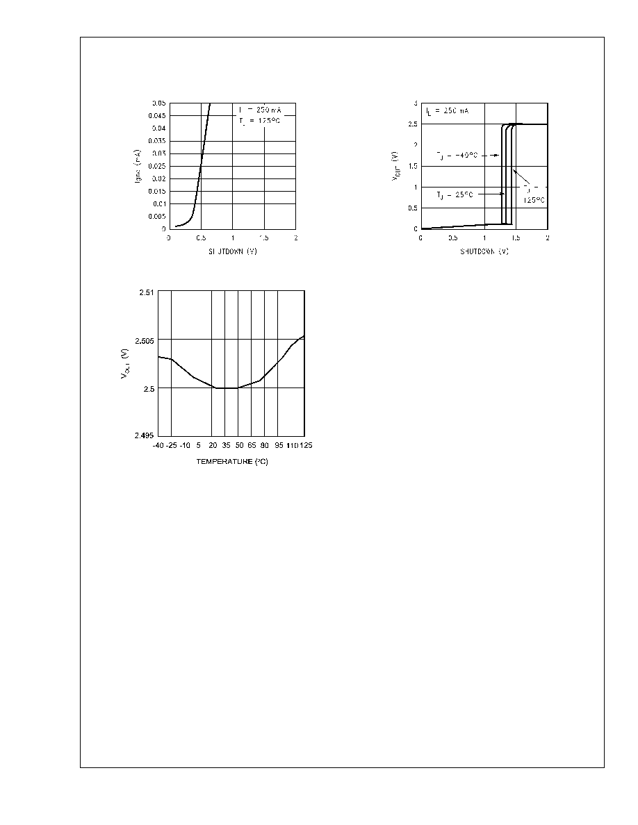
I
GND
vs Shutdown
10133931
10133910
I
GND
vs Shutdown
I
GND
vs Shutdown
10133908
10133909
LP2989
www.national.com
13
Typical Performance Characteristics
Unless otherwise specified: T
A
= 25∞C, C
OUT
= 4.7 µF,
C
IN
= 2.2 µF, S/D is tied to V
IN
, V
IN
= V
O
(NOM) + 1V, I
L
= 1 mA, V
OUT
= 2.5V. (Continued)
I
GND
vs Shutdown
V
OUT
vs Shutdown
10133907
10133924
Typical Temperature vs V
OUT
(LP2989-2.5)
10133955
LP2989
www.national.com
14

Application Hints
LLP Package Devices
The LP2989 is offered in the 8 lead LLP surface mount
package to allow for increased power dissipation compared
to the SO-8 and Mini SO-8. For details on thermal perfor-
mance as well as mounting and soldering specifications,
refer to Application Note AN-1187.
For output voltages
<
2V, see LP2989LV datasheet.
EXTERNAL CAPACITORS
Like any low-dropout regulator, the LP2989 requires external
capacitors for regulator stability. These capacitors must be
correctly selected for good performance.
INPUT CAPACITOR: An input capacitor whose size is at
least 2.2 µF is required between the LP2989 input and
ground (the amount of capacitance may be increased with-
out limit).
Characterization testing performed on the LP2989 has
shown that if the amount of actual input capacitance drops
below about 1.5 µF, an unstable operating condition may
result. Therefore, the next larger standard size (2.2 µF) is
specified as the minimum required input capacitance. Ca-
pacitor tolerance and temperature variation must be consid-
ered when selecting a capacitor (see Capacitor Character-
istics section) to assure the minimum requirement of 1.5 µF
is met over all operating conditions.
The input capacitor must be located at a distance of not
more than 0.5' from the input pin and returned to a clean
analog ground. Any good quality ceramic or tantalum may be
used for this capacitor, assuming the minimum capacitance
requirement is met.
OUTPUT CAPACITOR: The LP2989 requires a ceramic
output capacitor whose size is at least 4.7µF. The actual
amount of capacitance on the output must never drop below
about 3.5µF or unstable operation may result. For this rea-
son, capacitance tolerance and temperature characteristics
must be considered when selecting an output capacitor.
The LP2989 is designed specifically to work with ceramic
output capacitors, utilizing circuitry which allows the regula-
tor to be stable across the entire range of output current with
an output capacitor whose ESR is as low as 4 m
. It may
also be possible to use Tantalum or film capacitors at the
output, but these are not as attractive for reasons of size and
cost (see next section Capacitor Characteristics).
The output capacitor must meet the requirement for mini-
mum amount of capacitance and also have an ESR (equiva-
lent series resistance) value which is within the stable range.
Curves are provided which show the stable ESR range as a
function of load current (see ESR graph below).
10133938
Stable Region For output Capacitor ESR
Important: The output capacitor must maintain its ESR
within the stable region over the full operating temperature
range of the application to assure stability.
It is important to remember that capacitor tolerance and
variation with temperature must be taken into consideration
when selecting an output capacitor so that the minimum
required amount of output capacitance is provided over the
full operating temperature range. (See Capacitor Character-
istics section).
The output capacitor must be located not more than 0.5' from
the output pin and returned to a clean analog ground.
NOISE BYPASS CAPACITOR: Connecting a 10 nF capaci-
tor to the Bypass pin significantly reduces noise on the
regulator output. However, the capacitor is connected di-
rectly to a high-impedance circuit in the bandgap reference.
Because this circuit has only a few microamperes flowing in
it, any significant loading on this node will cause a change in
the regulated output voltage. For this reason, DC leakage
current through the noise bypass capacitor must never ex-
ceed 100 nA, and should be kept as low as possible for best
output voltage accuracy.
The types of capacitors best suited for the noise bypass
capacitor are ceramic and film. High-quality ceramic capaci-
tors with either NPO or COG dielectric typically have very
low leakage. 10 nF polypropolene and polycarbonate film
capacitors are available in small surface-mount packages
and typically have extremely low leakage current.
CAPACITOR CHARACTERISTICS
CERAMIC: The LP2989 was designed to work with ceramic
capacitors on the output to take advantage of the benefits
they offer: for capacitance values in the 4.7 µF range, ce-
ramics are the least expensive and also have the lowest
ESR values (which makes them best for eliminating
high-frequency noise). The ESR of a typical 4.7 µF ceramic
capacitor is in the range of 10 m
to 15 m, which easily
meets the ESR limits required for stability by the LP2989.
One disadvantage of ceramic capacitors is that their capaci-
tance can vary with temperature. Many large value ceramic
capacitors (
2.2 µF) are manufactured with the Z5U or Y5V
temperature characteristic, which results in the capacitance
dropping by more than 50% as the temperature goes from
25∞C to 85∞C.
This could cause problems if a 4.7 µF capacitor were used
on the output since it will drop down to approximately 2.4 µF
LP2989
www.national.com
15

Application Hints
(Continued)
at high ambient temperatures (which could cause the
LP2989 to oscillate). Another significant problem with Z5U
and Y5V dielectric devices is that the capacitance drops
severely with applied voltage. A typical Z5U or Y5V capacitor
can lose 60% of its rated capacitance with half of the rated
voltage applied to it.
For these reasons, X7R and X5R type ceramic capaci-
tors must be used on the input and output of the
LP2989.
TANTALUM: Tantalum capacitors are less desirable than
ceramics for use as output capacitors because they are
typically more expensive when comparing equivalent capaci-
tance and voltage ratings in the 1 µF to 4.7 µF range.
Another important consideration is that Tantalum capacitors
have higher ESR values than equivalent size ceramics. This
means that while it may be possible to find a Tantalum
capacitor with an ESR value within the stable range, it would
have to be larger in capacitance (which means bigger and
more costly) than a ceramic capacitor with the same ESR
value.
It should also be noted that the ESR of a typical Tantalum will
increase about 2:1 as the temperature goes from 25∞C down
to -40∞C, so some guard band must be allowed.
Tantalum capacitors may be used on the input as long as the
requirement for minimum capacitance is met.
FILM: Polycarbonate and polypropelene film capacitors
have excellent electrical performance: their ESR is the low-
est of the three types listed, their capacitance is very stable
with temperature, and DC leakage currrent is extremely low.
One disadvantage is that film capacitors are larger in physi-
cal size than ceramic or tantalum which makes film a poor
choice for either input or output capacitors.
However, their low leakage makes them a good choice for
the noise bypass capacitor. Since the required amount of
capacitance is only .01 µF, small surface-mount film capaci-
tors are avalable in this size.
SHUTDOWN INPUT OPERATION
The LP2989 is shut off by driving the Shutdown input low,
and turned on by pulling it high. If this feature is not to be
used, the Shutdown input should be tied to V
IN
to keep the
regulator output on at all times.
To assure proper operation, the signal source used to drive
the Shutdown input must be able to swing above and below
the specified turn-on/turn-off voltage thresholds listed in the
Electrical Characteristics section under V
ON/OFF
.
To prevent mis-operation, the turn-on (and turn-off) voltage
signals applied to the Shutdown input must have a slew rate
which is
40 mV/µs.
CAUTION: the regulator output voltage can not be guaran-
teed if a slow-moving AC (or DC) signal is applied that is in
the range between the specified turn-on and turn-off volt-
ages listed under the electrical specification V
ON/OFF
(see
Electrical Characteristics).
REVERSE INPUT-OUTPUT VOLTAGE
The PNP power transistor used as the pass element in the
LP2989 has an inherent diode connected between the regu-
lator output and input.
During normal operation (where the input voltage is higher
than the output) this diode is reverse-biased.
However, if the output is pulled above the input, this diode
will turn ON and current will flow into the regulator output.
In such cases, a parasitic SCR can latch which will allow a
high current to flow into V
IN
(and out the ground pin), which
can damage the part.
In any application where the output may be pulled above the
input, an external Schottky diode must be connected from
V
IN
to V
OUT
(cathode on V
IN
, anode on V
OUT
), to limit the
reverse voltage across the LP2989 to 0.3V (see Absolute
Maximum Ratings).
LP2989
www.national.com
16
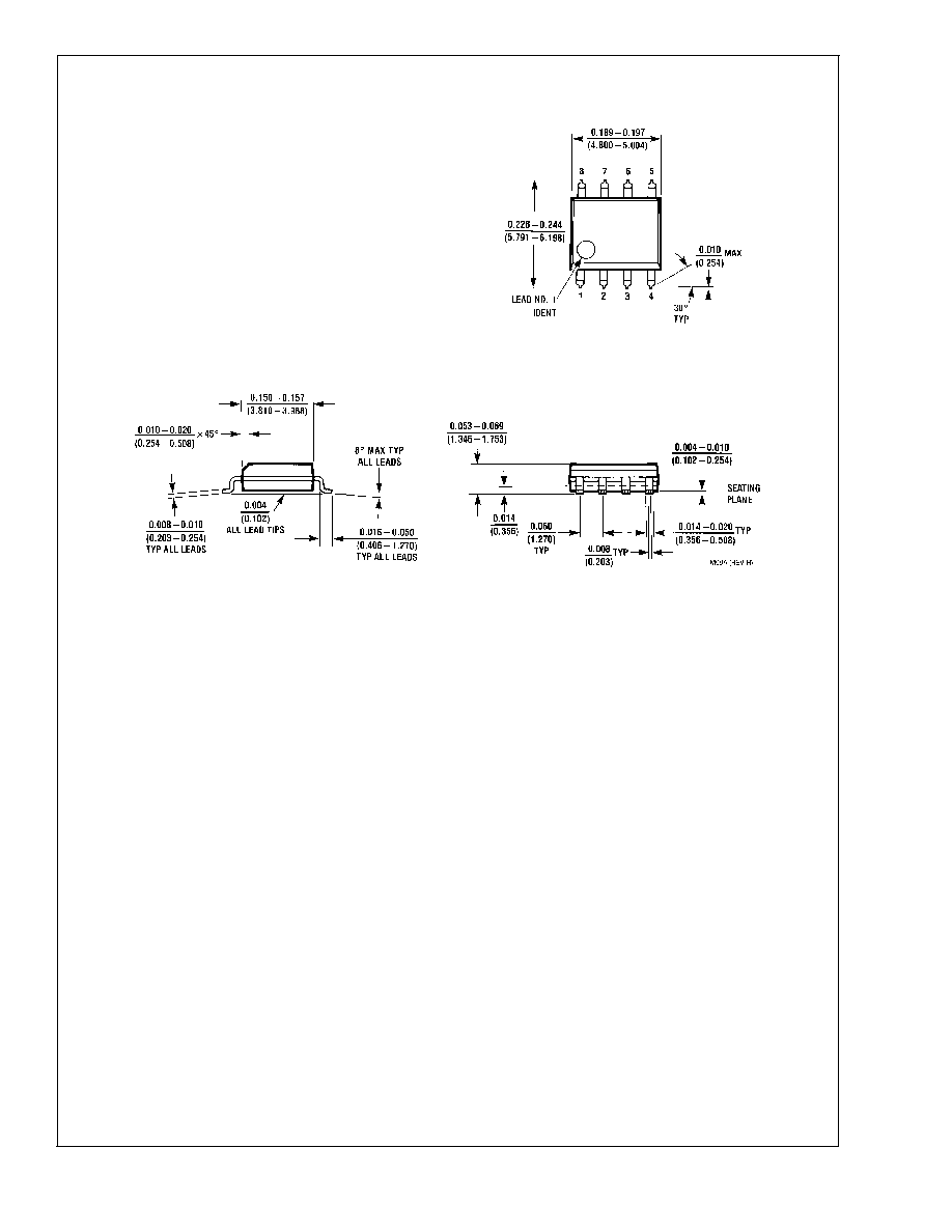
Physical Dimensions
inches (millimeters)
unless otherwise noted
SO-8 Package
NS Package Number M08A
LP2989
www.national.com
17
Physical Dimensions
inches (millimeters) unless otherwise noted (Continued)
Mini SO-8 Package
NS Package Number MUA08A
LP2989
www.national.com
18
Physical Dimensions
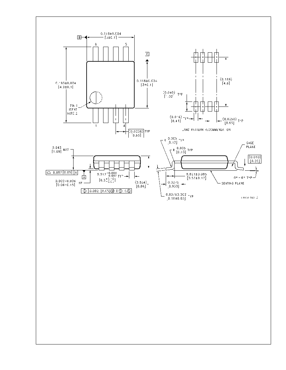
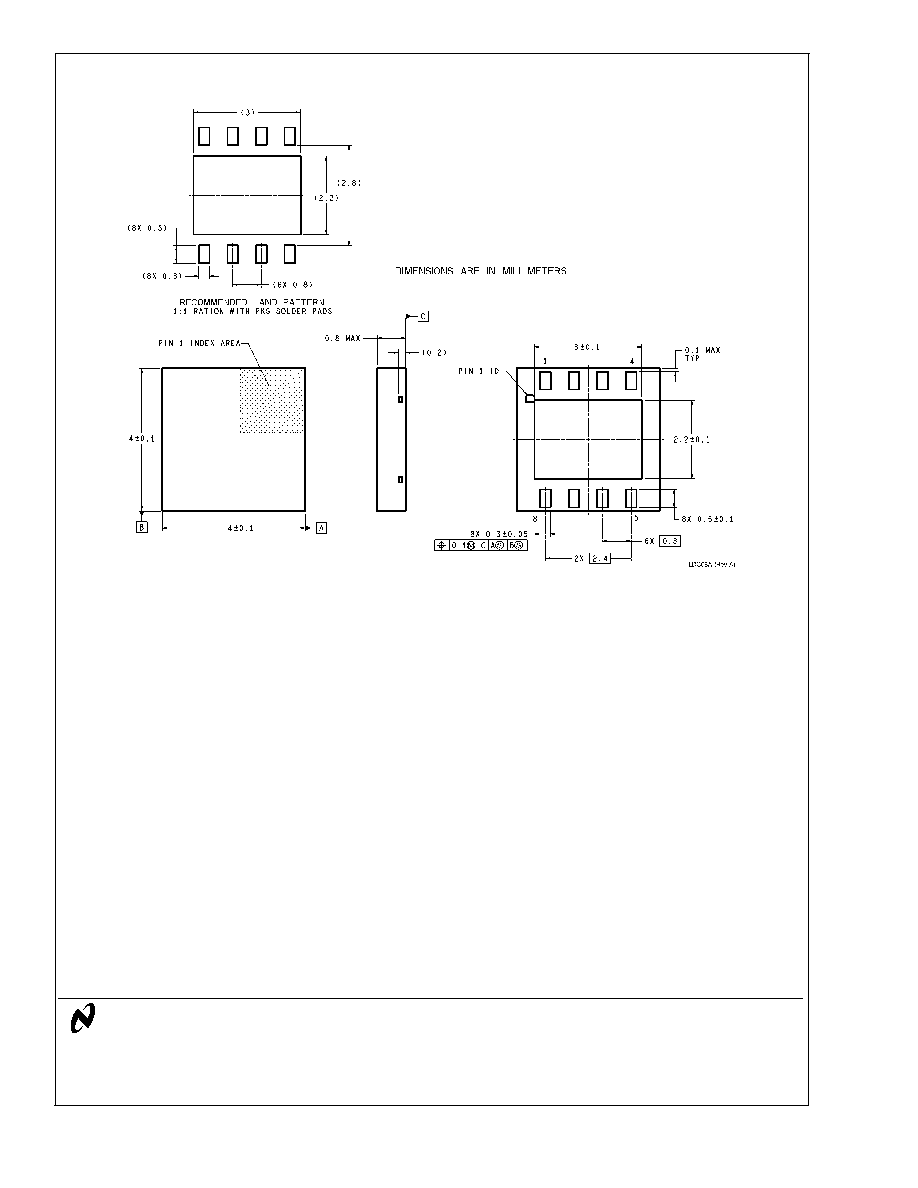
inches (millimeters) unless otherwise noted (Continued)
8 Lead LLP Surface Mount PackagePackage
NS Package Number LDC08A
LIFE SUPPORT POLICY
NATIONAL'S PRODUCTS ARE NOT AUTHORIZED FOR USE AS CRITICAL COMPONENTS IN LIFE SUPPORT
DEVICES OR SYSTEMS WITHOUT THE EXPRESS WRITTEN APPROVAL OF THE PRESIDENT AND GENERAL
COUNSEL OF NATIONAL SEMICONDUCTOR CORPORATION. As used herein:
1. Life support devices or systems are devices or
systems which, (a) are intended for surgical implant
into the body, or (b) support or sustain life, and
whose failure to perform when properly used in
accordance with instructions for use provided in the
labeling, can be reasonably expected to result in a
significant injury to the user.
2. A critical component is any component of a life
support device or system whose failure to perform
can be reasonably expected to cause the failure of
the life support device or system, or to affect its
safety or effectiveness.
National Semiconductor
Corporation
Americas
Email: support@nsc.com
National Semiconductor
Europe
Fax: +49 (0) 180-530 85 86
Email: europe.support@nsc.com
Deutsch Tel: +49 (0) 69 9508 6208
English
Tel: +44 (0) 870 24 0 2171
FranÁais Tel: +33 (0) 1 41 91 8790
National Semiconductor
Asia Pacific Customer
Response Group
Tel: 65-2544466
Fax: 65-2504466
Email: ap.support@nsc.com
National Semiconductor
Japan Ltd.
Tel: 81-3-5639-7560
Fax: 81-3-5639-7507
www.national.com
LP2989
Micropower/Low
Noise,
500
mA
Ultra
Low-Dropout
Regulator
For
Use
with
Ceramic
Output
Capacitors
National does not assume any responsibility for use of any circuitry described, no circuit patent licenses are implied and National reserves the right at any time without notice to change said circuitry and specifications.