LP2994
DDR Termination Regulator
General Description
The LP2994 regulator is designed to provide a linear solution
to meet the JEDEC SSTL-2 and SSTL-3 specifications (Se-
ries Stub Termination Logic) for active termination of DDR-
SDRAM. The device utilizes an internal operational amplifier
to provide linear regulation of V
TT
without the need for
expensive external components. The output stage prevents
shoot through while delivering 1.5A continuous current and
maintaining excellent load regulation. The LP2994 also in-
corporates an active low shutdown pin to tri-state the output
during Suspend To Ram (STR) states.
Patents Pending
Features
n
Source and sink current
n
Low external component count
n
Independent analog and power rails
n
Linear topology
n
Small package SO-8
n
Low cost and easy to use
n
Shutdown pin
Applications
n
SSTL-2
n
SSTL-3
n
DDR-SDRAM Termination
n
DDR-II Termination
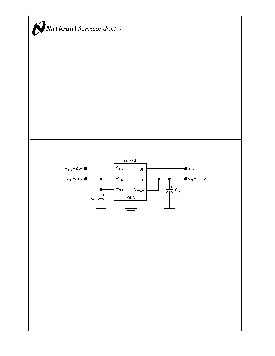
Typical Application Circuit
20045904
FIGURE 1. SSTL-2 V
TT
Termination
May 2002
LP2994
DDR
T
ermination
Regulator
© 2002 National Semiconductor Corporation
DS200459
www.national.com
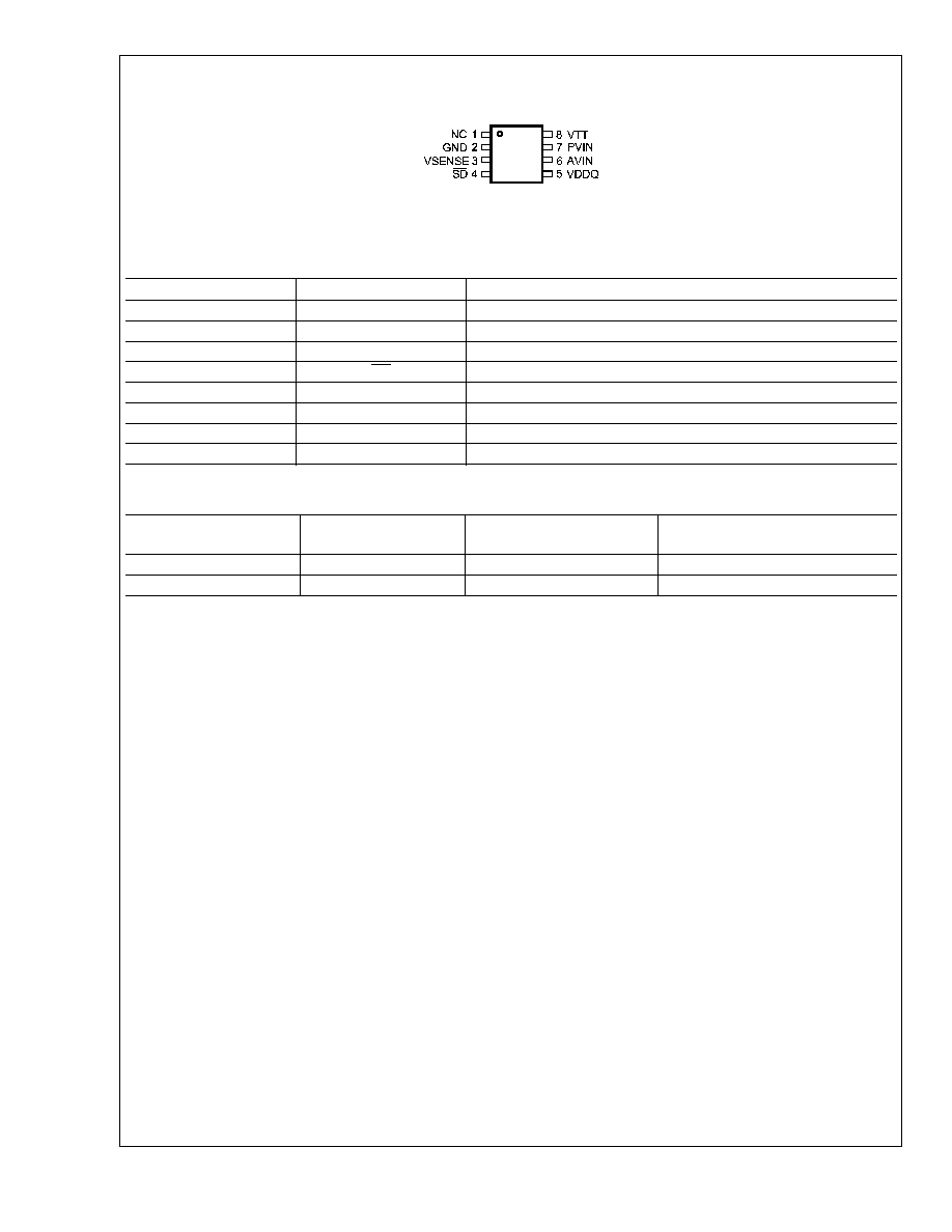
Absolute Maximum Ratings
(Note 1)
If Military/Aerospace specified devices are required,
please contact the National Semiconductor Sales Office/
Distributors for availability and specifications.
PVIN, AVIN, VTT, VDDQ, SD to GND
-0.3V to +6V
Storage Temp. Range
-65∞C to +150∞C
Junction Temperature
150∞C
Lead Temperature (Soldering, 10 sec)
260∞C
ESD Rating (Note 2)
2kV
Operating Range
Junction Temp. Range (Note 3)
0∞C to +125∞C
AVIN Supply Voltage
2.2V to 5.5V
PVIN Supply Voltage
-0.3V to (AVIN +
0.3V)
SD Input Voltage
-0.3V to (AVIN +
0.3V)
VTT Output Voltage
-0.3V to (PVIN +
0.3V)
SO-8 Thermal Resistance (
JA
)
151∞C/W
Electrical Characteristics
Specifications with standard typeface are for T
J
= 25∞C and limits in boldface
type apply over the full Operating Temperature Range (T
J
= 0∞C to +125∞C). Unless otherwise specified,
AVIN = PVIN = 2.5V, VDDQ = 2.5V (Note 4).
Symbol
Parameter
Conditions
Min
Typ
Max
Units
V
TT
V
TT
Output Voltage
I
OUT
= 0A (Note 5)
VIN=VDDQ = 2.3V
1.108
1.138
1.168
V
VIN=VDDQ = 2.5V
1.210
1.236
1.260
VIN=VDDQ = 2.7V
1.305
1.334
1.360
I
q
Quiescent Current
I
OUT
= 0A
(Note 6)
272
400
µA
Z
VDDQ
VDDQ Input Impedance
86
100
k
I
QSD
Quiescent current in
shutdown
21
45
µA
I
SD
Shutdown Leakage
Current
SD = 0V
SD = 2.5V
2
2
5
µA
nA
V
IH
Minimum Shutdown High
Level
1.9
V
V
IL
Maximum Shutdown Low
Level
0.8
V
V
TT
/V
TT
Load Regulation
(Note 7)
I
OUT
= 0 to 1.5A
-0.4
%
I
OUT
= 0 to -1.5A
+0.4
I
SENSE
SENSE Input Current
100
pA
Note 1: Absolute maximum ratings indicate limits beyond which damage to the device may occur. Operating range indicates conditions for which the device is
intended to be functional, but does not guarantee specific performance limits. For guaranteed specifications and test conditions see Electrical Characteristics. The
guaranteed specifications apply only for the test conditions listed. Some performance characteristics may degrade when the device is not operated under the listed
test conditions.
Note 2: The human body model is a 100pF capacitor discharged through a 1.5k
resistor into each pin.
Note 3: At elevated temperatures, devices must be derated based on thermal resistance. The device in the SO-8 package must be derated at
JA
= 151.2∞ C/W
junction to ambient with no heat sink.
Note 4: Limits are 100% production tested at 25∞C. Limits over the operating temperature range are guaranteed through correlation using Statistical Quality Control
(SQC) methods. The limits are used to calculate National's Average Outgoing Quality Level (AOQL).
Note 5: VIN is defined as the VIN = AVIN = PVIN
Note 6: Quiescent current defined as the current flow into AVIN.
Note 7: Load regulation is tested by using a 10ms current pulse and measuring V
TT
.
LP2994
www.national.com
3
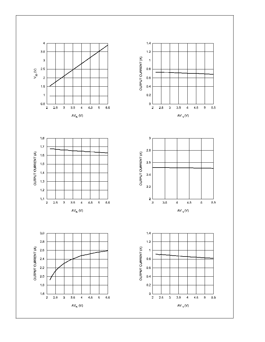
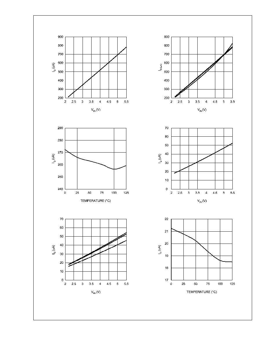
Typical Performance Characteristics
(Continued)
V
IL
and V
IH
vs AV
IN
(25∞C)
Maximum Sourcing Current vs AV
IN
(V
DDQ
= 2.5V, PV
IN
= 1.8V)
20045920
20045921
Maximum Sourcing Current vs AV
IN
(V
DDQ
= 2.5V, PV
IN
= 2.5V)
Maximum Sourcing Current vs AV
IN
(V
DDQ
= 2.5V, PV
IN
= 3.3V)
20045922
20045923
Maximum Sinking Current vs AV
IN
(V
DDQ
= 2.5V)
Maximum Sourcing Current vs AV
IN
(V
DDQ
= 1.8V, PV
IN
= 1.8V)
20045924
20045925
LP2994
www.national.com
5