LP2996
DDR Termination Regulator
General Description
The LP2996 linear regulator is designed to meet the JEDEC
SSTL-2 specifications for termination of DDR-SDRAM. The
device contains a high-speed operational amplifier to provide
excellent response to load transients. The output stage pre-
vents shoot through while delivering 1.5A continuous current
and transient peaks up to 3A in the application as required
for DDR-SDRAM termination. The LP2996 also incorporates
a V
SENSE
pin to provide superior load regulation and a V
REF
output as a reference for the chipset and DIMMs.
An additional feature found on the LP2996 is an active low
shutdown (SD) pin that provides Suspend To RAM (STR)
functionality. When SD is pulled low the V
TT
output will
tri-state providing a high impedance output, but, V
REF
will
remain active. A power savings advantage can be obtained
in this mode through lower quiescent current.
Features
n
Source and sink current
n
Low output voltage offset
n
No external resistors required
n
Linear topology
n
Suspend to Ram (STR) functionality
n
Low external component count
n
Thermal Shutdown
n
Available in SO-8, PSOP-8 or LLP-16 packages
Applications
n
DDR-I and DDR-II Termination Voltage
n
SSTL-2 and SSTL-3 Termination
n
HSTL Termination
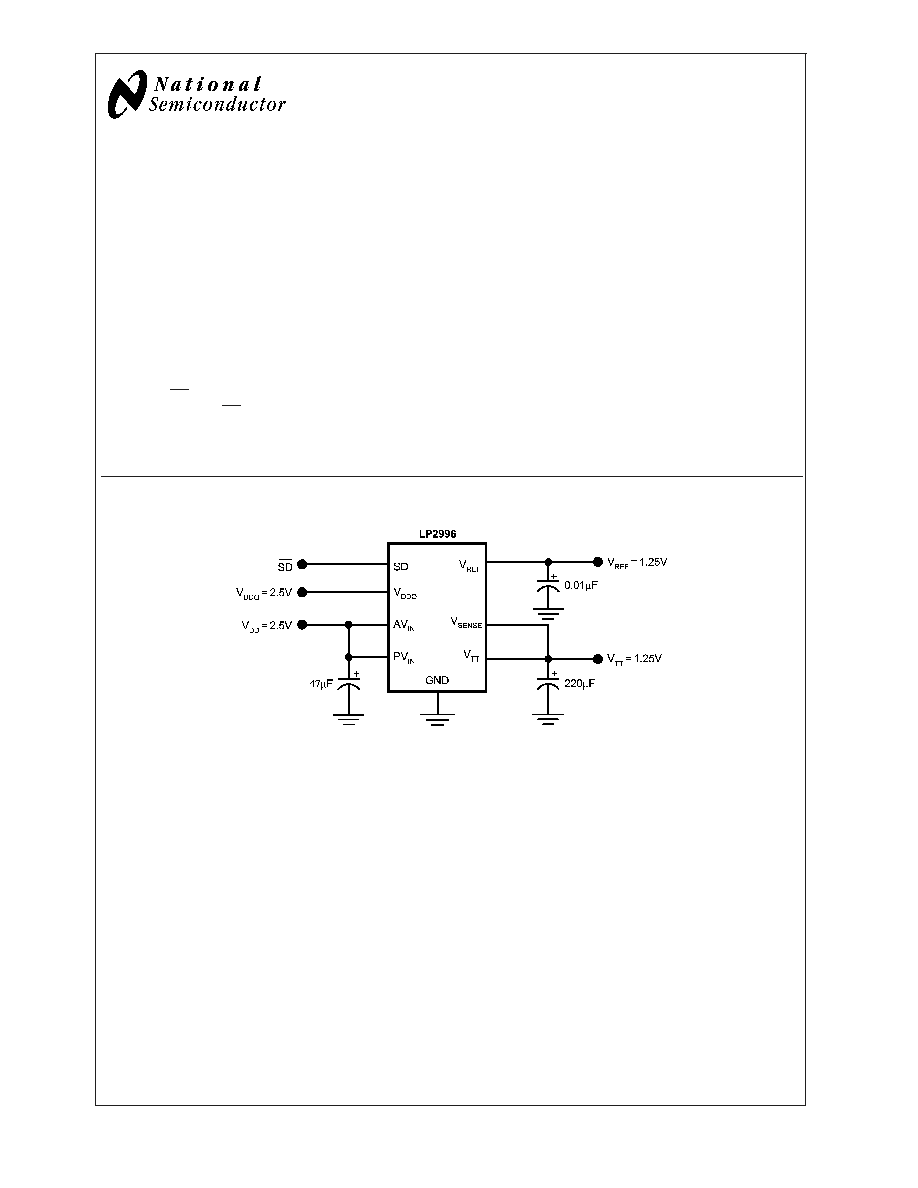
Typical Application Circuit
20057518
December 2002
LP2996
DDR
T
ermination
Regulator
� 2002 National Semiconductor Corporation
DS200575
www.national.com
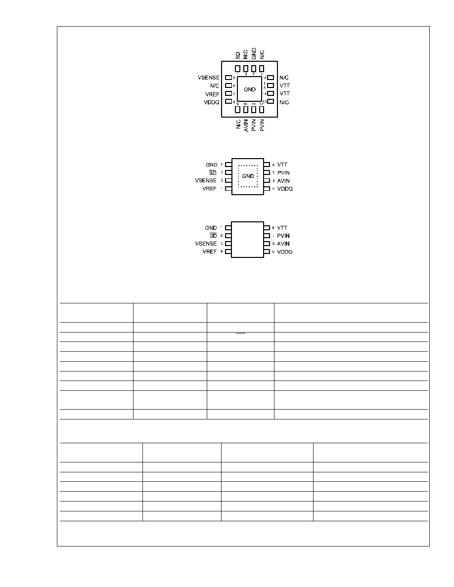
Connection Diagrams
20057502
LLP-16 Layout
20057503
PSOP-8 Layout
20057504
SO-8 Layout
Pin Description
SO-8 Pin or
PSOP-8 Pin
LLP Pin
Name
Function
1
2
GND
Ground
2
4
SD
Shutdown
3
5
VSENSE
Feedback pin for regulating V
TT
.
4
7
VREF
Buffered internal reference voltage of V
DDQ
/2
5
8
VDDQ
Input for internal reference equal to V
DDQ
/2
6
10
AVIN
Analog input pin
7
11, 12
PVIN
Power input pin
8
14, 15
VTT
Output voltage for connection to termination
resistors
-
1, 3, 6, 9, 13, 16
NC
No internal connection
Ordering Information
Order Number
Package Type
NSC Package
Drawing
Supplied As
LP2996M
SO-8
M08A
95 Units per Rail
LP2996MX
SO-8
M08A
2500 Units Tape and Reel
LP2996MR
PSOP-8
MRA08A
95 Units Tape and Reel
LP2996MRX
PSOP-8
MRA08A
2500 Units Tape and Reel
LP2996LQ
LLP-16
LQA16A
1000 Units Tape and Reel
LP2996LQX
LLP-16
LQA16A
4500 Units Tape and Reel
LP2996
www.national.com
2
Absolute Maximum Ratings
(Note 1)
If Military/Aerospace specified devices are required,
please contact the National Semiconductor Sales Office/
Distributors for availability and specifications.
PVIN, AVIN, VDDQ to GND
-0.3V to +6V
Storage Temp. Range
-65�C to +150�C
Junction Temperature
150�C
SO-8 Thermal Resistance (
JA
)
151�C/W
PSOP-8 Thermal Resistance (
JA
)
43�C/W
LLP-16 Thermal Resistance (
JA
)
51�C/W
Lead Temperature (Soldering, 10 sec)
260�C
ESD Rating (Note 2)
1kV
Operating Range
Junction Temp. Range (Note 3)
0�C to +125�C
AVIN to GND
2.2V to 5.5V
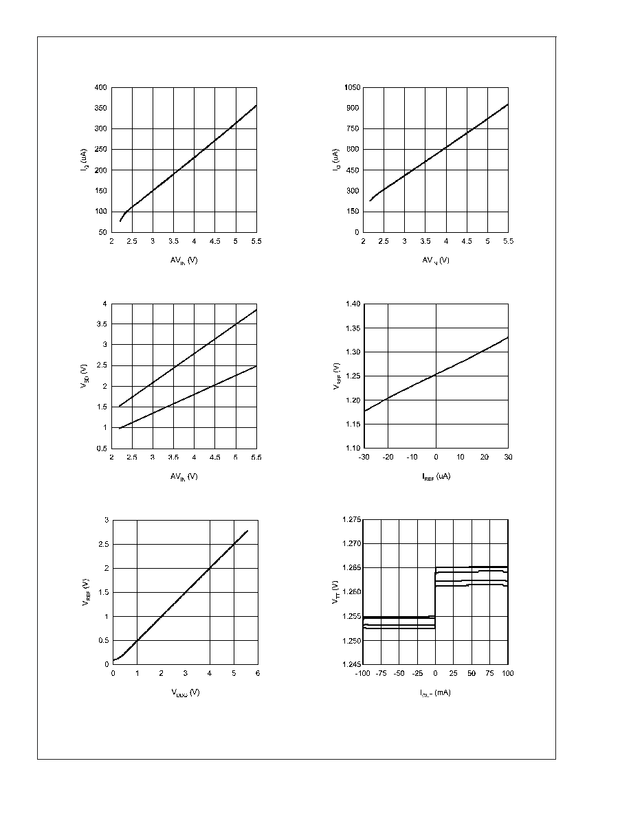
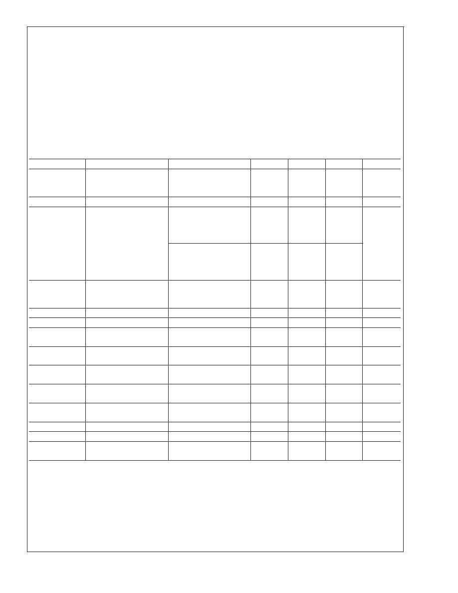
Electrical Characteristics
Specifications with standard typeface are for T
J
= 25�C and limits in boldface
type apply over the full Operating Temperature Range (T
J
= 0�C to +125�C) (Note 4). Unless otherwise specified,
AVIN = PVIN = 2.5V, VDDQ = 2.5V (Note 5).
Symbol
Parameter
Conditions
Min
Typ
Max
Units
V
REF
V
REF
Voltage
VIN = VDDQ = 2.3V
VIN = VDDQ = 2.5V
VIN = VDDQ = 2.7V
1.135
1.235
1.335
1.158
1.258
1.358
1.185
1.285
1.385
V
Z
VREF
V
REF
Output Impedance
I
REF
= -30 to +30 �A
2.5
k
V
TT
V
TT
Output Voltage
I
OUT
= 0A
VIN = VDDQ = 2.3V
VIN = VDDQ = 2.5V
VIN = VDDQ = 2.7V
1.125
1.225
1.325
1.159
1.259
1.359
1.190
1.290
1.390
V
I
OUT
=
�
1.5A (Note 8)
VIN = VDDQ = 2.3V
VIN = VDDQ = 2.5V
VIN = VDDQ = 2.7V
1.125
1.225
1.325
1.159
1.259
1.359
1.190
1.290
1.390
Vos
TT
/V
TT
V
TT
Output Voltage Offset
(V
REF
-V
TT
)
I
OUT
= 0A
I
OUT
= -1.5A (Note 8)
I
OUT
= +1.5A (Note 8)
-20
-25
-25
0
0
0
20
25
25
mV
I
Q
Quiscent Current (Note 6)
I
OUT
= 0A (Note 4)
320
500
�A
Z
VDDQ
VDDQ Input Impedance
100
k
I
SD
Quiescent Current in
Shutdown (Note 6)
SD = 0V
115
150
�A
I
Q_SD
Shutdown Leakage
Current
SD = 0V
2
5
�A
V
IH
Minimum Shutdown High
Level
1.9
V
V
IL
Minimum Shutdown Low
Level
0.8
V
I
V
V
TT
Leakage Current in
Shutdown
SD = 0V
V
TT
= 1.25V
1
10
�A
I
SENSE
V
SENSE
Input Current
13
nA
T
SD
Thermal Shutdown
(Note 7)
165
Celcius
T
SD
_HYS
Thermal Shutdown
Hysteresis
10
Celcius
LP2996
www.national.com
3

Electrical Characteristics
Specifications with standard typeface are for T
J
= 25�C and limits in boldface type
apply over the full Operating Temperature Range (T
J
= 0�C to +125�C) (Note 4). Unless otherwise specified,
AVIN = PVIN = 2.5V, VDDQ = 2.5V (Note 5). (Continued)
Note 1: Absolute maximum ratings indicate limits beyond which damage to the device may occur. Operating range indicates conditions for which the device is
intended to be functional, but does not guarantee specific performance limits. For guaranteed specifications and test conditions see Electrical Characteristics. The
guaranteed specifications apply only for the test conditions listed. Some performance characteristics may degrade when the device is not operated under the listed
test conditions.
Note 2: The human body model is a 100pF capacitor discharged through a 1.5k
resistor into each pin.
Note 3: At elevated temperatures, devices must be derated based on thermal resistance. The device in the SO-8 package must be derated at
JA
= 151.2� C/W
junction to ambient with no heat sink.
Note 4: Limits are 100% production tested at 25�C. Limits over the operating temperature range are guaranteed through correlation using Statistical Quality Control
(SQC) methods. The limits are used to calculate National's Average Outgoing Quality Level (AOQL).
Note 5: VIN is defined as VIN = AVIN = PVIN.
Note 6: Quiescent current defined as the current flow into AVIN.
Note 7: The maximum allowable power dissipation is a function of the maximum junction temperature, T
J(MAX)
, the junction to ambient thermal resistance,
JA
, and
the ambient temperature, T
A
. Exceeding the maximum allowable power dissipation will cauyse excessive die temperature and the regulator will go into thermal
shutdown.
Note 8: V
TT
load regulation is tested by using a 10 ms current pulse and measuring V
TT
.
LP2996
www.national.com
4