TL H 5711
LP311
Voltage
Comparator
February 1995
LP311 Voltage Comparator
General Description
The LP311 is a low power version of the industry-standard
LM311 It takes advantage of stable high-value ion-implant-
ed resistors to perform the same function as an LM311 with
a 30 1 reduction in power drain but only a 6 1 slowdown of
response time Thus the LP311 is well suited for battery-
powered applications and all other applications where fast
response is not needed It operates over a wide range of
supply voltages from 36V down to a single 3V supply with
less than 200 mA drain but it is still capable of driving a 25
mA load The LP311 is quite easy to apply without any oscil-
lation if ordinary precautions are taken to minimize stray
coupling from the output to either input or to the balance
pins (as described in the LM311 datasheet Application
Hints)
Features
Y
Low power drain 900 mW on 5V supply
Y
Operates from
g
15V or a single supply as low as 3V
Y
Output can drive 25 mA
Y
Emitter output can swing below negative supply
Y
Response time 1 2 ms
Y
Same pin-out as LM311
Y
Low input currents 2 nA of offset 15 nA of bias
Y
Large common-mode input range
b
14 6V to 13 6V
with
g
15V supply
Applications
Y
Level-detector for battery-powered instruments
Y
Low-power lamp or relay driver
Y
Low-power zero-crossing detector
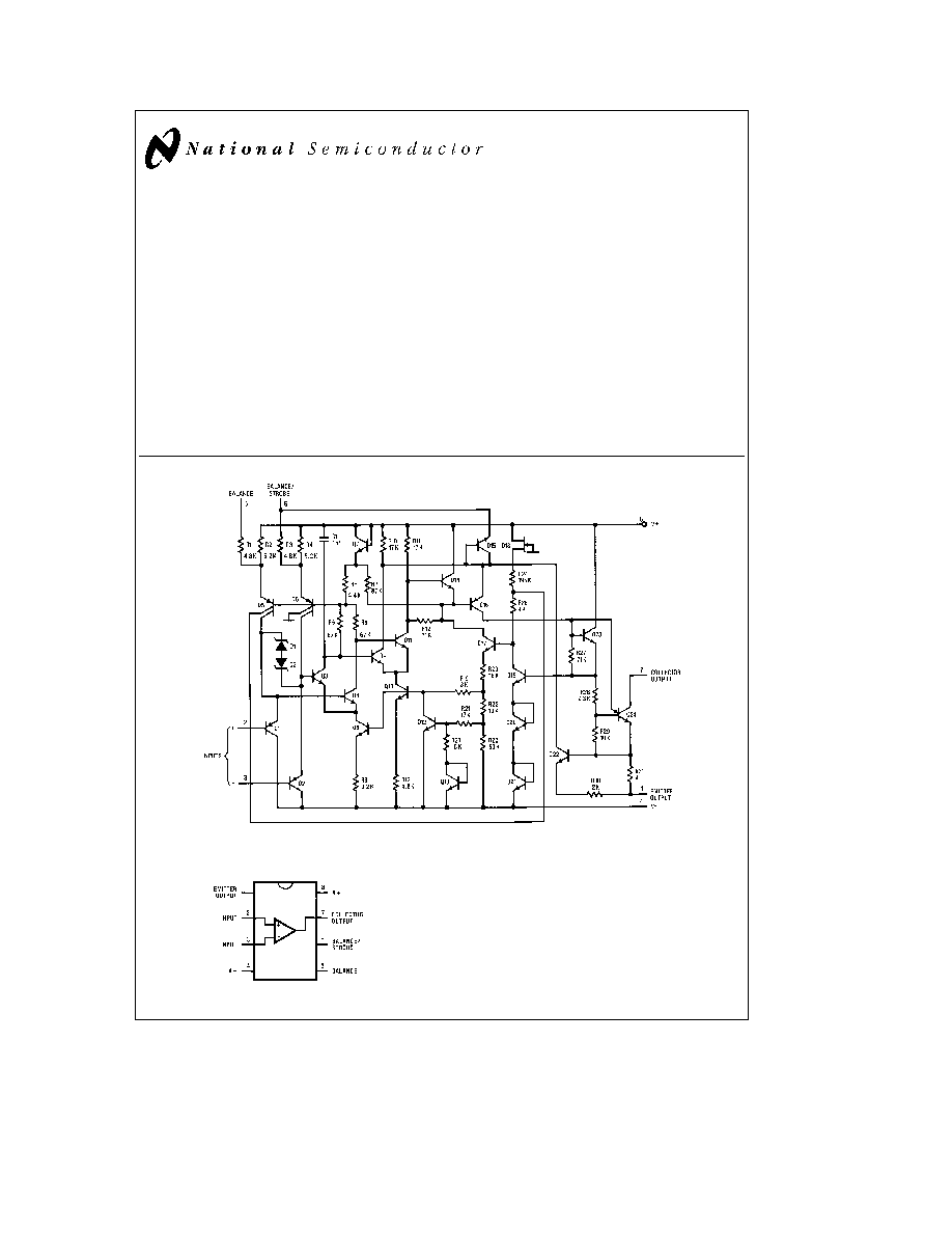
Schematic Diagram
TL H 5711 ≠ 7
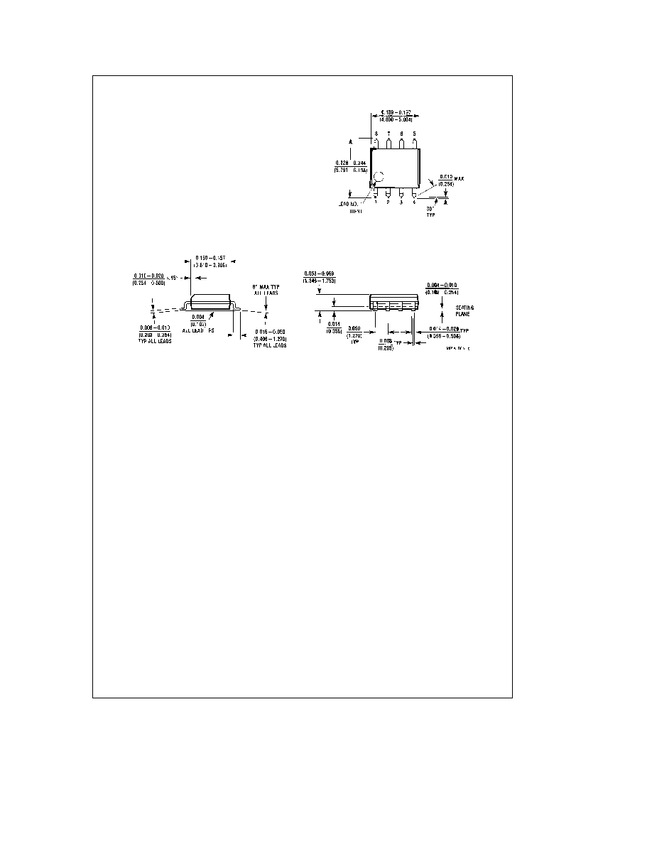
Connection Diagram
Dual-In-Line Package
TL H 5711 ≠ 4
Top View
Order Number LP311M or LP311N
See NS Package Numbers M08A or N08E
C1995 National Semiconductor Corporation
RRD-B30M115 Printed in U S A
Absolute Maximum Ratings
If Military Aerospace specified devices are required
please contact the National Semiconductor Sales
Office Distributors for availability and specifications
Total Supply Voltage (V
8 ≠ 4
)
36V
Collector Output to Negative Supply Voltage (V
7 ≠ 4
)
40V
Collector Output to Emitter Output
40V
Emitter Output to Negative Supply Voltage (V
1 ≠ 4
)
g
30V
Differential Input Voltage
g
30V
Input Voltage (Note 1)
g
15V
Power Dissipation (Note 2)
500 mW
Output Short Circuit Duration
10 sec
Operating Temperature Range
0 C to 70 C
Storage Temperature Range
b
65 C to 150 C
Lead Temperature (Soldering 10 seconds)
260 C
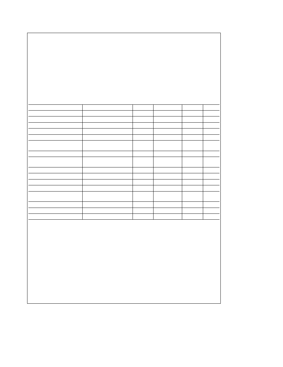
Electrical Characteristics
These specifications apply for V
S
e
g
15V and 0 C
s
T
A
s
70 C unless otherwise specified
Parameter
Conditions
Min
Typ
Max
Units
Input Offset Voltage (Notes 3 4)
T
A
e
25 C R
S
s
100k
2 0
7 5
mV
Input Offset Current (Notes 3 4)
T
A
e
25 C
2 0
25
nA
Input Bias Current (Note 3)
T
A
e
25 C
15
100
nA
Voltage Gain
T
A
e
25 C R
L
e
5k
40
200
V mV
Response Time (Note 5)
T
A
e
25 C
1 2
m
s
Saturation Voltage (Note 6)
V
IN
s
b
10 mV I
OUT
e
25 mA
0 4
1 5
V
T
Ae25 C
Strobe Current (Note 7)
T
A
e
25 C
100
200
300
m
A
Output Leakage Current
V
IN
t
10 mV V
OUT
e
35V
0 2
100
nA
T
A
e
25 C
Input Offset Voltage (Notes 3 4)
R
S
s
100k
10
mV
Input Offset Current (Notes 3 4)
35
nA
Input Bias Current (Note 3)
150
nA
Input Voltage Range
V
b
a
0 5
a
13 7
b
14 7
V
a
b
1 5
V
Saturation Voltage (Note 6)
V
a t
4 5V V
b
e
0V
0 1
0 4
V
V
IN
s
b
10 mV I
SINK
s
1 6 mA
Positive Supply Current
T
A
e
25 C Output on
150
300
m
A
Negative Supply Current
T
A
e
25 C
80
180
m
A
Minimum Operating Voltage
T
A
e
25 C
3 0
3 5
V
Note 1
This rating applies for
g
15V supplies The positive input voltage limit is 30V above the negative supply The negative input voltage limit is equal to the
negative supply voltage or 30V below the positive supply whichever is less
Note 2
The maximum junction temperature of the LP311 is 85 C For operating at elevated temperatures devices in the dual-in-line package must be derated
based on a thermal resistance of 160 C W junction to ambient
Note 3
The offset voltage offset current and bias current specifications apply for any supply voltage from a single 4V supply up to
g
15V supplies
Note 4
The offset voltages and offset currents given are the maximum values required to drive the output within a volt of either supply with 1 mA load Thus these
parameters define an error band and take into account the worst-case effects of voltage gain and input impedance
Note 5
The response time specified is for a 100 mV input step with 5 mV overdrive
Note 6
Saturation voltage specification applies to collector-emitter voltage (V7-1) for V
COLLECTOR
s
(V
a
b
3V)
Note 7
This specification gives the range of current which must be drawn from the strobe pin to ensure the output is properly disabled Do not short the strobe pin
to ground It should be current driven 100 mA to 300 mA
2
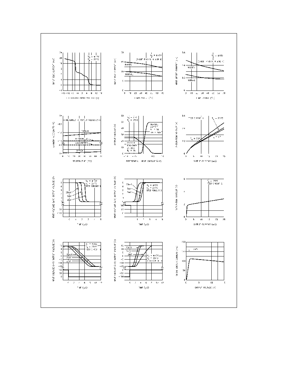
Typical Performance Characteristics
Input Characteristics
Input Bias Current
Input Offset Current
Common Mode Limits
Transfer Function
Output Saturation Voltage
(Collector Output)
Response Time for Various
Input Overdrives
Response Time for Various
Input Overdrives
Output Saturation Voltage
(Emitter Output)
Response Time for Various
Input Overdrives
Response Time for Various
Input Overdrives
Output Limiting
Characteristics
TL H 5711 ≠ 5
3
Typical Performance Characteristics
(Continued)
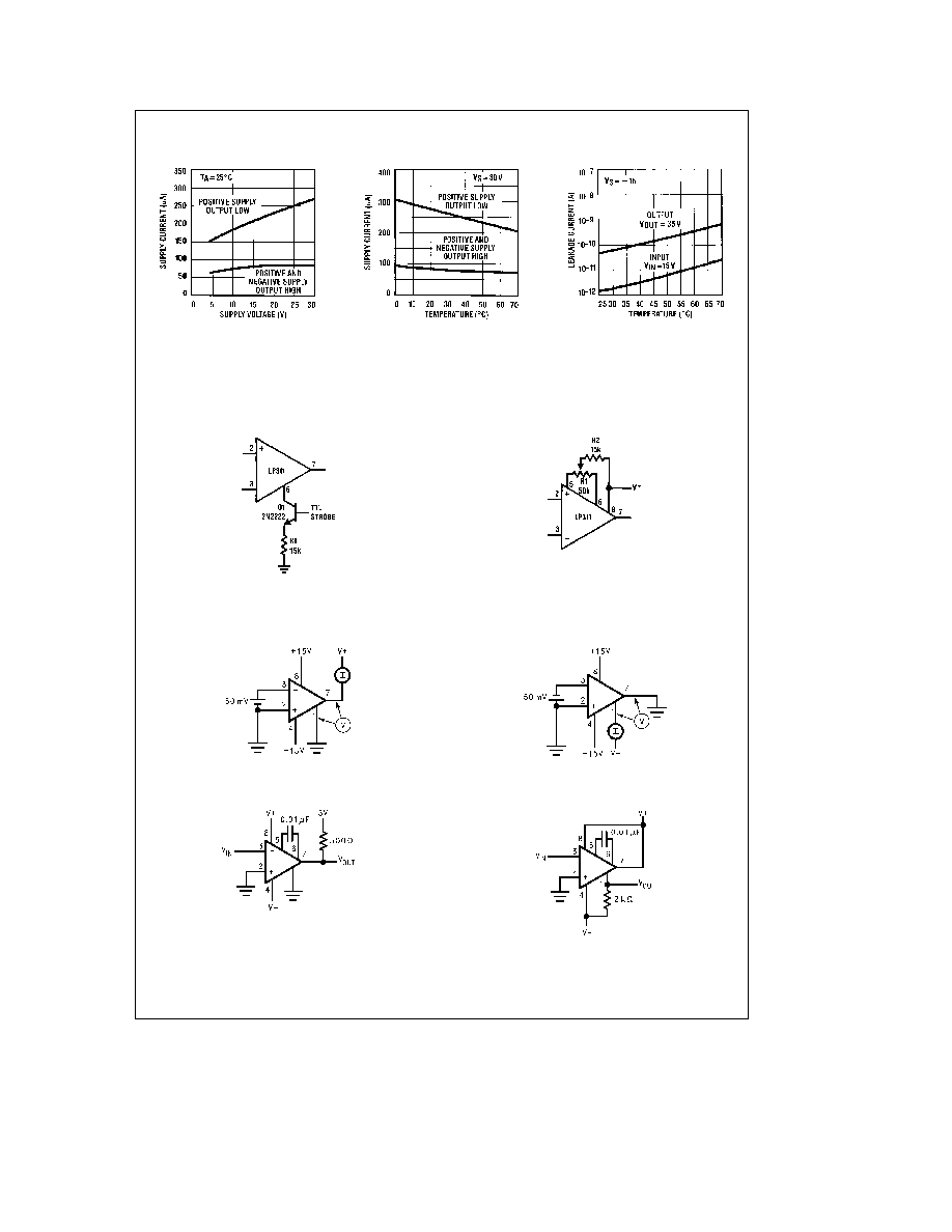
Supply Current
Supply Current
Leakage Currents
TL H 5711 ≠ 6
Applications Information
For applications information and typical applications refer to the LM311 datasheet
Auxiliary Circuits
Strobing
TL H 5711 ≠ 1
Note
Do not ground strobe pin
Offset Balancing
TL H 5711 ≠ 2
Test Circuits
Test Circuit 1 (Collector Output)
TL H 5711 ≠ 8
Test Circuit 2 (Emitter Output)
TL H 5711 ≠ 9
Test Circuit 3 (Collector Output)
TL H 5711 ≠ 10
Test Circuit 4 (Emitter Output)
TL H 5711 ≠ 11
4