LP324/LP2902
Micropower Quad Operational Amplifier
General Description
The LP324 series consists of four independent, high gain
internally compensated micropower operational amplifiers.
These amplifiers are specially suited for operation in battery
systems while maintaining good input specifications, and
extremely low supply current drain. In addition, the LP324
has an input common mode range, and output source range
which includes ground, making it ideal in single supply ap-
plications.
These amplifiers are ideal in applications which include por-
table instrumentation, battery backup equipment, and other
circuits which require good DC performance and low supply
current.
Features
n
Low supply current:
85µA (typ)
n
Low offset voltage:
2mV (typ)
n
Low input bias current:
2nA (typ)
n
Input common mode to GND
n
Interfaces to CMOS logic
n
Wide supply range:
3V
<
V
+
<
32V
n
Small Outline Package available
n
Pin-for-pin compatible with LM324
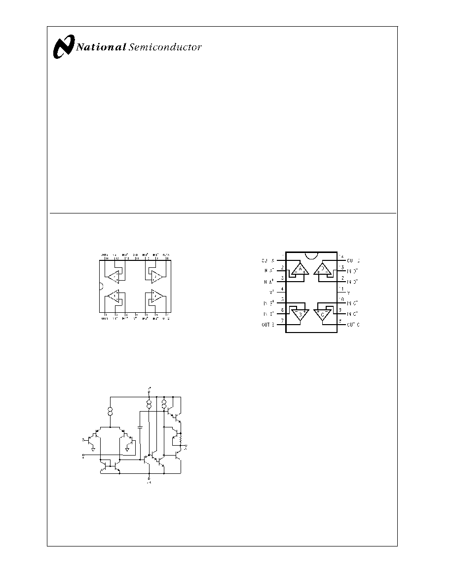
Connection Diagrams
Dual-In-Line (N) and SO (M)
14-Pin TSSOP
00856201
Order Number LP324M or LP2902M
See NS Package Number M14A
Order Number LP324N or LP2902N
See NS Package Number N14A
00856240
Order Number LP324MT and LP324MTX
See NS Package Number MTC14
Simplified Schematic
00856202
July 2001
LP324/LP2902
Micropower
Quad
Operational
Amplifier
© 2001 National Semiconductor Corporation
DS008562
www.national.com
Absolute Maximum Ratings
(Note 1)
If Military/Aerospace specified devices are required,
please contact the National Semiconductor Sales Office/
Distributors for availability and specifications.
Supply Voltage
LP324
32V or
±
16V
LP2902
26V or
±
13V
Differential Input Voltage
LP324
32V
LP2902
26V
Input Voltage (Note 2)
LP324
-0.3V to 32V
LP2902
-0.3V to 26V
Output Short-Circuit to GND
Continuous
(One Amplifier) (Note 3)
V
+
15V and T
A
= 25∞C
ESD Susceptibility (Note 10)
±
500V
Operating Conditions
T
JMAX
150∞C
JA
(Note 4)
MT Package
154∞C/W
N Package
90∞C/W
M Package
140∞C/W
Operating Temp. Range
(Note 5)
Storage Temp. Range
-65∞C
T
J
150∞C
Soldering Information
Wave Soldering(10sec)
260∞C(lead temp.)
Convection or Infrared(20sec)
235∞C
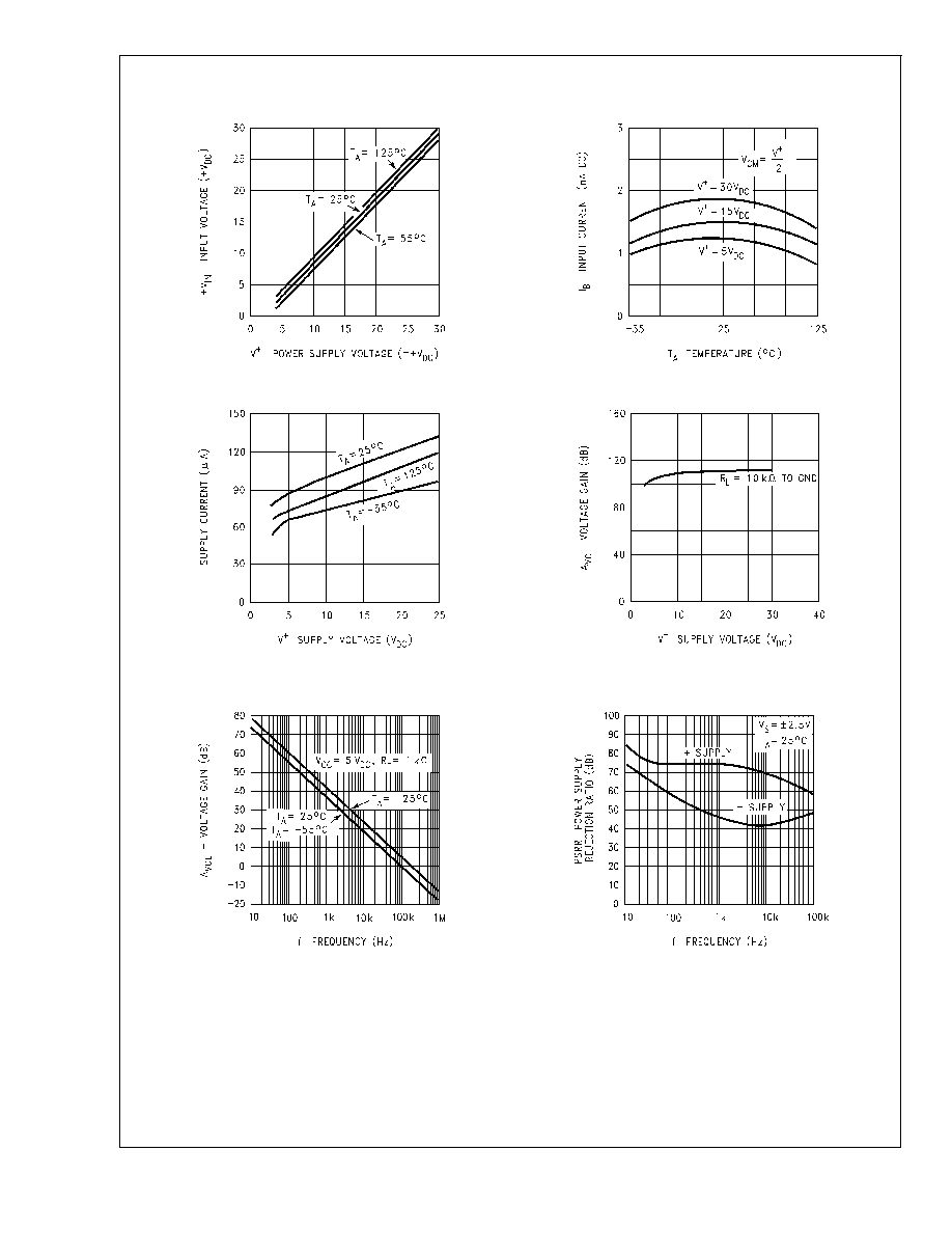
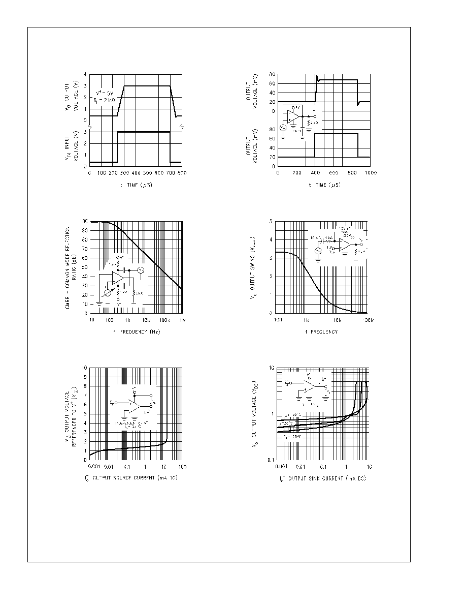
Electrical Characteristics
(Note 6)
LP2902 (Note 9)
LP324
Symbol
Parameter
Conditions
Tested
Design
Tested
Design
Units
Typ
Limit
Limit
Typ
Limit
Limit
Limits
(Note 7)
(Note 8)
(Note 7)
(Note 8)
V
OS
Input Offset
Voltage
2
4
10
2
4
9
mV
(Max)
I
B
Input Bias Current
2
20
40
2
10
20
nA
(Max)
I
OS
Input Offset Current
0.5
4
8
0.2
2
4
nA
(Max)
A
VOL
Voltage Gain
R
L
= 10k to GND
V
+
= 30V
70
40
30
100
50
40
V/mV
(Min)
CMRR
Common Mode Rej.
Ratio
V
+
= 30V, 0V
V
CM
V
CM
<
V
+
- 1.5
90
80
75
90
80
75
dB
(Min)
PSRR
Power Supply Rej.
Ratio
V
+
= 5V to 30V
90
80
75
90
80
75
dB
(Min)
I
S
Supply Current
R
L
=
85
150
250
85
150
250
µA
(Max)
V
O
Output Voltage
Swing
I
L
= 350µA to GND
V
CM
= 0V
3.6
3.4
V
+
-1.9V
3.6
3.4
V
+
-1.9V
V
(Min)
I
L
= 350µA to V
+
V
CM
= 0V
0.7
0.8
1.0
0.7
0.8
1.0
V
(Max)
I
OUT
Source
Output Source
Current
V
O
= 3V
V
IN
(diff) = 1V
10
7
4
10
7
4
mA
(Min)
I
OUT
Sink
Output Sink Current
V
O
= 1.5V
V
IN
(diff) = 1V
5
4
3
5
4
3
mA
(Min)
I
OUT
Sink
Output Sink Current
V
O
= 1.5V
V
CM
= 0V
4
2
1
4
2
1
mA
(Min)
I
SOURCE
Output Short to GND
V
IN
(diff) = 1V
20
25
35
35
20
25
35
35
mA
(Max)
I
SINK
Output Short to V
+
V
IN
(diff) = 1V
15
30
45
15
30
45
mA
(Max)
V
OS
Drift
10
10
µV/C∞
I
OS
Drift
10
10
pA/C∞
LP324/LP2902
www.national.com
2
Electrical Characteristics
(Note 6) (Continued)
LP2902 (Note 9)
LP324
Symbol
Parameter
Conditions
Tested
Design
Tested
Design
Units
Typ
Limit
Limit
Typ
Limit
Limit
Limits
(Note 7)
(Note 8)
(Note 7)
(Note 8)
GBW
Gain Bandwidth
Product
100
100
KHz
SR
Slew Rate
50
50
V/mS
Note 1: "Absolute Maximum Ratings" indicate limits beyond which damage to the device may occur. Operating Ratings indicate conditions for which the device is
functional, but do not guarantee specific performance limits.
Note 2: The input voltage is not allowed to go more than -0.3V below V
-
(GND) as this will turn on a parasitic transistor causing large currents to flow through the
device.
Note 3: Short circuits from the output to GND can cause excessive heating and eventual destruction. The maximum sourcing output current is approximately 30 mA
independent of the magnitude of V
+
. At values of supply voltage in excess of 15 V
DC
, continuous short-circuit to GND can exceed the power dissipation ratings
(particularly at elevated temperatures) and cause eventual destruction. Destructive dissipation can result from simultaneous shorts on all amplifiers.
Note 4: For operation at elevated temperatures, these devices must be derated based on a thermal resistance of
JA
and T
J
max. T
J
= T
A
+
JA
P
D
.
Note 5: The LP2902 may be operated from -40∞C
T
A
+85∞C, and the LP324 may be operated from 0∞C
T
A
+70∞C.
Note 6: Boldface numbers apply at temperature extremes. All other numbers apply only at T
A
= T
J
= 25∞C, V
+
= 5V, V
cm
= V/2, and R
L
=100k connected to GND
unless otherwise specified.
Note 7: Guaranteed and 100% production tested.
Note 8: Guaranteed (but not 100% production tested) over the operating supply voltage range (3.0V to 32V for the LP324, LP324, and 3.0V to 26V for the LP2902),
and the common mode range (0V to V
+
-1.5V), unless otherwise specified. These limits are not used to calculate outgoing quality levels.
Note 9: The LP2902 operating supply range is 3V to 26V, and is not tested above 26V.
Note 10: The test circuit used consists of the human body model of 100 pF in series with 1500
.
LP324/LP2902
www.national.com
3