 | –≠–ª–µ–∫—Ç—Ä–æ–Ω–Ω—ã–π –∫–æ–º–ø–æ–Ω–µ–Ω—Ç: LP339N | –°–∫–∞—á–∞—Ç—å:  PDF PDF  ZIP ZIP |
LP339
Ultra-Low Power Quad Comparator
General Description
The LP339 consists of four independent voltage compara-
tors designed specifically to operate from a single power
supply and draw typically 60 µA of power supply drain cur-
rent over a wide range of power supply voltages. Operation
from split supplies is also possible and the ultra-low power
supply drain current is independent of the power supply volt-
age. These comparators also feature a common-mode
range which includes ground, even when operated from a
single supply.
Applications
include
limit
comparators,
simple
analog-to-digital converters, pulse, square and time delay
generators; VCO's; multivibrators; high voltage logic gates.
The LP339 was specifically designed to interface with the
CMOS logic family. The ultra-low supply current makes the
LP339 valuable in battery powered applications.
Advantages
n
Ultra-low power supply drain suitable for battery
applications
n
Single supply operation
n
Sensing at ground
n
Compatible with CMOS logic family
n
Pin-out identical to LM339
Features
n
Ultra-low power supply current drain
(60 µA) -- independent of the supply voltage
(75 µW/comparator at +5 V
DC
)
n
Low input biasing current:
3 nA
n
Low input offset current:
±
0.5 nA
n
Low input offset voltage:
±
2 mV
n
Input common-mode voltage includes ground
n
Output voltage compatible with MOS and CMOS logic
n
High output sink current capability (30 mA at V
O
=2 V
DC
)
n
Supply Input protected against reverse voltages
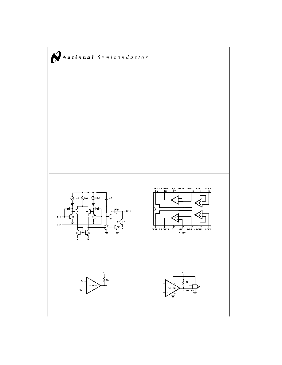
Schematic and Connection Diagrams
Typical Applications
(V
+
= 5.0 V
DC
)
DS005226-1
DS005226-2
Order Number LP339M for S.O. Package
See NS Package Number M14A
Order Number LP339N for Dual-In-Line Package
See NS Package Number N14A
Basic Comparator
DS005226-3
Driving CMOS
DS005226-4
September 1999
LP339
Ultra-Low
Power
Quad
Comparator
© 1999 National Semiconductor Corporation
DS005226
www.national.com
Absolute Maximum Ratings
(Note 1)
If Military/Aerospace specified devices are required,
please contact the National Semiconductor Sales Office/
Distributors for availability and specifications.
Supply Voltage
36 V
DC
or
±
18 V
DC
Differential Input Voltage
±
36 V
DC
Input Voltage
-0.3 V
DC
to 36 V
DC
Power Dissipation (Note 2)
Molded DIP
570 mW
Output Short Circuit to GND (Note 3)
Continuous
Input Current V
IN
<
-0.3 V
DC
(Note 4)
50 mA
Operating Temperature Range
0∞C to +70∞C
Storage Temperature Range
-65∞ to +150∞C
Soldering Information:
Dual-In-Line Package (10 sec.)
+260∞C
S.O. Package:
Vapor Phase (60 sec.)
+215∞C
Infrared (15 sec.)
+220∞C
See AN-450 "Surface Mounting Methods and Their Effect on
Product Reliability" for other methods of soldering surface
mount devices.
Electrical Characteristics
(V+=5 V
DC
) (Note 5)
Parameter
Conditions
Min
Typ
Max
Units
Input Offset Voltage
T
A
=25∞C (Note 10)
±
2
±
5
mV
DC
Input Bias Current
I
IN
(+) or I
IN
(-) with the
2.5
25
nA
DC
Output in the Linear Range, T
A
=25∞C (Note 6)
Input Offset Current
I
IN
(+)-I
IN
(-), T
A
=25∞C
±
0.5
±
5
nA
DC
Input Common
T
A
=25∞C (Note 7)
0
V+-1.5
V
DC
Mode Voltage Range
Supply Current
R
L
=Infinite on all Comparators, T
A
=25∞C
60
100
µA
DC
Voltage Gain
V
O
= 1 V
DC
to 11 V
DC
,
500
V/mV
R
L
=15 k
, V
+
=15 V
DC
, T
A
=25∞C
Large Signal
V
IN
=TTL Logic Swing, V
REF
=1.4 V
DC
,
1.3
µSec
Response Time
V
RL
=5 V
DC
, R
L
=5.1 k
, T
A
=25∞C
Response Time
V
RL
=5 V
DC
, R
L
=5.1 k
, T
A
=25∞C (Note 8)
8
µSec
Output Sink Current
V
IN
(-)=1 V
DC
, V
IN
(+)=0, V
O
=2 V
DC
,
15
30
mA
DC
T
A
=25∞C (Note 12)
V
O
=0.4 V
DC
0.20
0.70
mA
DC
Output Leakage Current
V
IN
(+)=1 V
DC
, V
IN
(-)=0, V
O
=5 V
DC
, T
A
=25∞C
0.1
nA
DC
Input Offset Voltage
(Note 10)
±
9
mV
DC
Input Offset Current
I
IN
(+)-I
IN
(-)
±
1
±
15
nA
DC
Input Bias Current
I
IN
(+) or I
IN
(-) with Output in Linear Range
4
40
nA
DC
Input Common
Single Supply
0
V+-2.0
V
DC
Mode Voltage Range
Output Sink Current
V
IN
(-)=1 V
DC
, V
IN
(+)=0, V
O
=2 V
DC
10
mA
DC
Output Leakage Current
V
IN
(+)=1 V
DC
, V
IN
(-)=0, V
O
=30 V
DC
1.0
µA
DC
Differential Input Voltage
All V
IN's
0 V
DC
(or V
-
on split supplies) (Note 9)
36
V
DC
Note 1: Absolute Maximum Ratings indicate limits beyond which damage to the device may occur. Operating Ratings indicate conditions for which the device is func-
tional, but do not guarantee specific performance limits.
Note 2: For elevated temperature operation, T
j
max is 125∞C for the LP339.
ja
(junction to ambient) is 175∞C/W for the LP339N and 120∞C/W for the LP339M when
either device is soldered in a printed circuit board in a still air environment. The low bias dissipation and the "ON-OFF" characteristic of the outputs keeps the chip
dissipation very small (P
D
100 mW), provided the output transistors are allowed to saturate.
Note 3: Short circuits from the output to V
+
can cause excessive heating and eventual destruction. The maximum output current is approximately 50 mA.
Note 4: This input current will only exist when the voltage at any of the input leads is driven negative. It is due to the collector-base junction of the input PNP tran-
sistors becoming forward biased and thereby acting as input clamp diodes. In addition to this diode action, there is also lateral NPN parasitic transistor action on the
IC chip. This transistor action can cause the output voltage of the comparators to go to the V+ voltage level (or to ground for a large input overdrive) for the time du-
ration that an input is driven negative. This is not destructive and normal output states will re-establish when the input voltage, which is negative, again returns to a
value greater than -0.3 V
DC
(T
A
=25∞C).
Note 5: These specifications apply for V
+
=5V
DC
and 0∞C
T
A
70∞ C, unless otherwise stated. The temperature extremes are guaranteed but not 100% production
tested. These parameters are not used to calculate outgoing AQL.
Note 6: The direction of the input current is out of the IC due to the PNP input stage. This current is essentially constant, independent of the state of the output, so
no loading change exists on the reference or the input lines as long as the common-mode range is not exceeded.
Note 7: The input common-mode voltage or either input voltage should not be allowed to go negative by more than 0.3V. The upper end of the common-mode volt-
age range is V
+
-1.5V (T
A
=25∞C), but either or both inputs can go to 30 V
DC
without damage.
Note 8: The response time specified is for a 100 mV input step with 5 mV overdrive. For larger overdrive signals 1.3 µs can be obtained. See Typical Performance
Characteristics section.
www.national.com
2
Electrical Characteristics
(Continued)
Note 9: Positive excursions of input voltage may exceed the power supply level. As long as the other voltage remains within the common-mode range, the compara-
tor will provide a proper output state. The low input voltage state must not be less than -0.3 V
DC
(or 0.3 V
DC
below the magnitude of the negative power supply, if
used) at T
A
=25∞C.
Note 10: At output switch point, V
O
=1.4V, R
S
=0
with V
+
from 5 V
DC
; and over the full input common-mode range (0 V
DC
to V
+
-1.5 V
DC
).
Note 11: For input signals that exceed V
+
, only the overdriven comparator is affected. With a 5V supply, V
IN
should be limited to 25V maximum, and a limiting resistor
should be used on all inputs that might exceed the positive supply.
Note 12: The output sink current is a function of the output voltage. The LP339 has a bi-modal output section which allows it to sink large currents via a Darlington
connection at output voltages greater than approximately 1.5 V
DC
and sink lower currents below this point. (See typical characteristics section and applications sec-
tion).
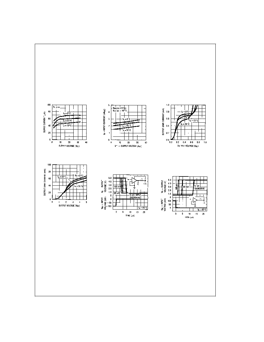
Typical Performance Characteristics
Supply Current
DS005226-35
Input Current
DS005226-36
Output Sink Current
DS005226-37
Output Sink Current
DS005226-38
Response Times for
Various Input
Overdrives --
Negative Transition
DS005226-39
Response Times for
Various Input
Overdrives --
Positive Transition
DS005226-40
www.national.com
3
Application Hints
All pins of any unused comparators should be tied to the
negative supply.
The bias network of the LP339 establishes a drain current
which is independent of the magnitude of the power supply
voltage over the range of from 2 V
DC
to 30 V
DC
.
It is usually unnecessary to use a bypass capacitor across
the power supply line.
The differential input voltage may be larger than V+ without
damaging the device. Protection should be provided to pre-
vent the input voltages from going negative more than -0.3
V
DC
(at 25∞C). An input clamp diode can be used as shown
in the application section.
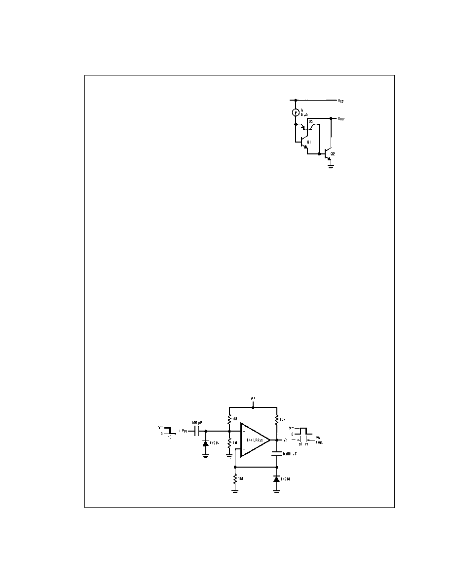
The output section of the LP339 has two distinct modes of
operation-a Darlington mode and a grounded emitter mode.
This unique drive circuit permits the LP339 to sink 30 mA at
V
O
=2 V
DC
(Darlington mode) and 700 µA at V
O
=0.4 V
DC
(grounded emitter mode).
Figure 1 is a simplified schematic
diagram of the LP339 output section.
Notice that the output section is configured in a Darlington
connection (ignoring Q3). Therefore, if the output voltage is
held high enough (V
O
1 V
DC
), Q1 is not saturated and the
output current is limited only by the product of the betas of
Q1, Q2 and I1 (and the 60
R
SAT
of Q2). The LP339 is thus
capable of driving LED's, relays, etc. in this mode while
maintaining an ultra-low power supply current of typically
60 µA.
If transistor Q3 were omitted, and the output voltage allowed
to drop below about 0.8 V
DC
, transistor Q1 would saturate
and the output current would drop to zero. The circuit would,
therefore, be unable to "pull" low current loads down to
ground (or the negative supply, if used). Transistor Q3 has
been included to bypass transistor Q1 under these condi-
tions and apply the current I1 directly to the base of Q2. The
output sink current is now approximately I1 times the beta of
Q2 (700 µA at V
O
=0.4 V
DC
). The output of the LP339 exhib-
its a bi-modal characteristic with a smooth transition be-
tween modes. (See Output Sink Current graphs in Typical
Performance Characteristics section.)
It is also important to note that in both cases the output is an
uncommitted collector. Therefore, many collectors can be
tied together to provide an output OR'ing function. An output
pull-up resistor can be connected to any available power
supply voltage within the permitted power supply voltage
range and there is no restriction on this voltage due to the
magnitude of the voltage which is applied to the V+ terminal
of the LP339 package.
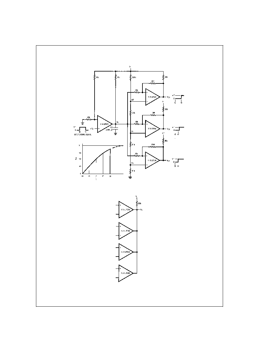
Typical Applications
(V
+
=15 V
DC
)
DS005226-11
FIGURE 1.
One-Shot Multivibrator
DS005226-13
www.national.com
4
Typical Applications
(V
+
=15 V
DC
) (Continued)
Time-Delay Generator
DS005226-15
ORing the Outputs
DS005226-16
www.national.com
5
Typical Applications
(V
+
=15 V
DC
) (Continued)
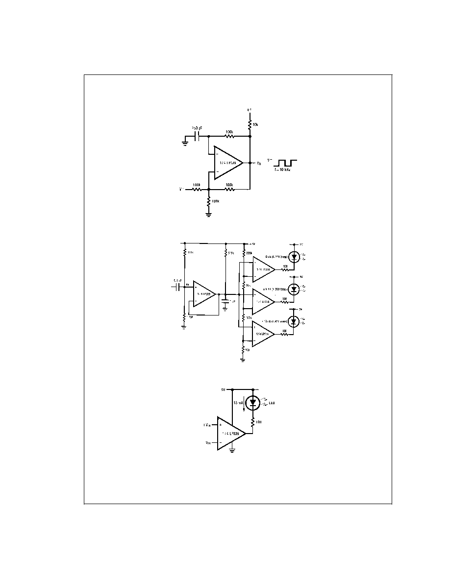
Squarewave Oscillator
DS005226-17
Three Level Audio Peak Indicator
DS005226-19
LED Driver
DS005226-22
www.national.com
6
Typical Applications
(V
+
=15 V
DC
) (Continued)
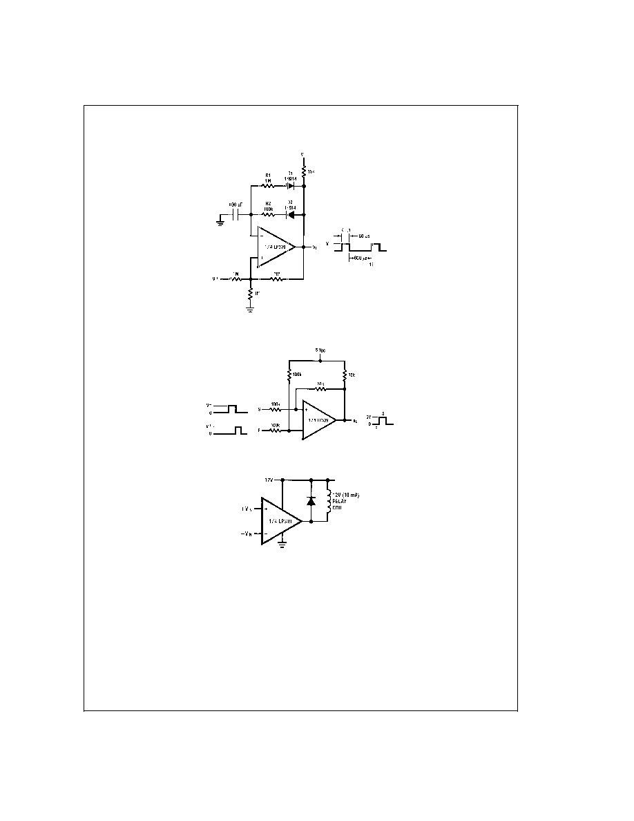
Pulse Generator
DS005226-18
Bi-Stable Multivibrator
DS005226-21
Relay Driver
DS005226-23
www.national.com
7
Typical Applications
(V
+
=15 V
DC
) (Continued)
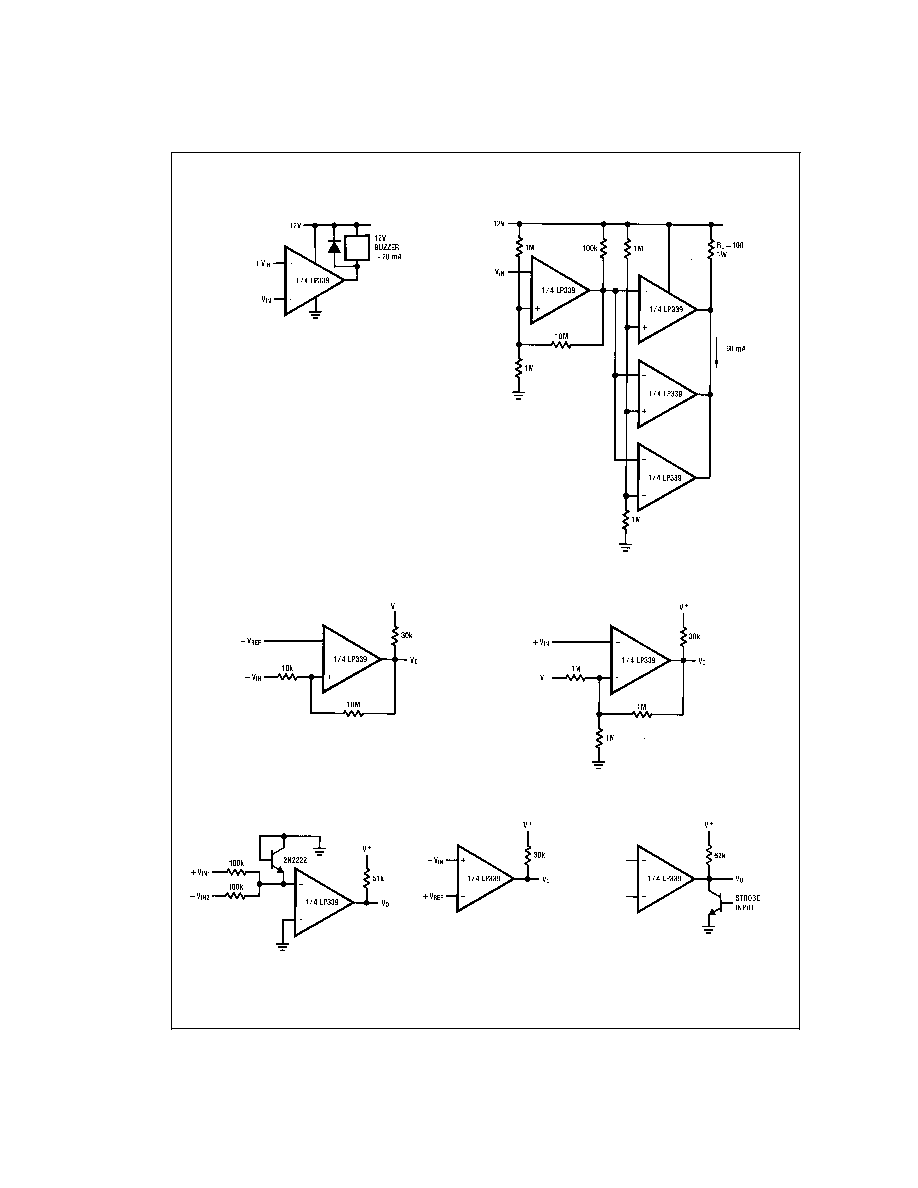
Buzzer Driver
DS005226-24
Comparator With 60 mA Sink Capability
DS005226-25
Non-Inverting Comparator with Hysteresis
DS005226-26
Inverting Comparator with Hysteresis
DS005226-27
Comparing Input Voltages
of Opposite Polarity
DS005226-28
Basic Comparator
DS005226-29
Output Strobing
DS005226-30
www.national.com
8

Typical Applications
(V
+
=15 V
DC
) (Continued)
Transducer Amplifier
DS005226-31
Zero Crossing Detector (Single Power Supply)
DS005226-32
Split-Supply Applications
Zero Crossing Detector
DS005226-33
Comparator With a Negative Reference
DS005226-34
www.national.com
9
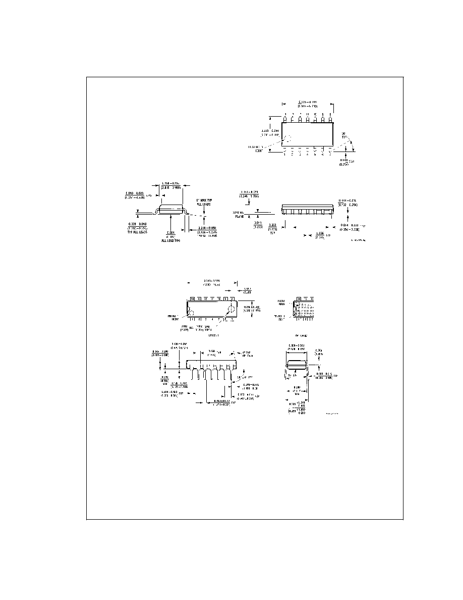
Physical Dimensions
inches (millimeters) unless otherwise noted
S.O. Package (M)
Order Number LP339M
NS Package M14A
Molded Dual-In-Line Package (N)
Order Number LP339N
NS Package Number N14A
www.national.com
10
Notes
LIFE SUPPORT POLICY
NATIONAL'S PRODUCTS ARE NOT AUTHORIZED FOR USE AS CRITICAL COMPONENTS IN LIFE SUPPORT
DEVICES OR SYSTEMS WITHOUT THE EXPRESS WRITTEN APPROVAL OF THE PRESIDENT AND GENERAL
COUNSEL OF NATIONAL SEMICONDUCTOR CORPORATION. As used herein:
1. Life support devices or systems are devices or
systems which, (a) are intended for surgical implant
into the body, or (b) support or sustain life, and
whose failure to perform when properly used in
accordance with instructions for use provided in the
labeling, can be reasonably expected to result in a
significant injury to the user.
2. A critical component is any component of a life
support device or system whose failure to perform
can be reasonably expected to cause the failure of
the life support device or system, or to affect its
safety or effectiveness.
National Semiconductor
Corporation
Americas
Tel: 1-800-272-9959
Fax: 1-800-737-7018
Email: support@nsc.com
National Semiconductor
Europe
Fax: +49 (0) 1 80-530 85 86
Email: europe.support@nsc.com
Deutsch Tel: +49 (0) 1 80-530 85 85
English
Tel: +49 (0) 1 80-532 78 32
FranÁais Tel: +49 (0) 1 80-532 93 58
Italiano
Tel: +49 (0) 1 80-534 16 80
National Semiconductor
Asia Pacific Customer
Response Group
Tel: 65-2544466
Fax: 65-2504466
Email: sea.support@nsc.com
National Semiconductor
Japan Ltd.
Tel: 81-3-5639-7560
Fax: 81-3-5639-7507
www.national.com
LP339
Ultra-Low
Power
Quad
Comparator
National does not assume any responsibility for use of any circuitry described, no circuit patent licenses are implied and National reserves the right at any time without notice to change said circuitry and specifications.