LP3470
Tiny Power On Reset Circuit
General Description
The LP3470 is a micropower CMOS voltage supervisory cir-
cuit designed to monitor power supplies in microprocessor
(µP) and other digital systems. It provides maximum adjust-
ability for power-on-reset (POR) and supervisory functions. It
is available in the following six standard reset threshold volt-
age (V
RTH
) options: 2.63V, 2.93V, 3.08V, 4.00V, 4.38V, and
4.63V. If other voltage options between 2.4V and 5.0V are
desired please contact your National Semiconductor repre-
sentative.
The LP3470 asserts a reset signal whenever the V
CC
supply
voltage falls below a reset threshold. The reset time-out pe-
riod is adjustable using an external capacitor. Reset remains
asserted for an interval (programmed by an external capaci-
tor) after V
CC
has risen above the threshold voltage.
The device is available in the tiny SOT23-5 package.
Key Specifications
n
±
1% Reset Threshold Accuracy Over Temperature
n
Standard Reset Threshold Voltages: 2.63V, 2.93V,
3.08V, 4.00V, 4.38V, and 4.63V
n
Custom Reset Threshold Voltages: For other voltages
between 2.4V and 5.0V contact your National
Semiconductor representative
n
Very Low Quiescent Current (16 µA typical)
n
Guaranteed Reset valid down to V
CC
=0.5V
Features
n
Tiny SOT23-5 Package
n
Open Drain Reset Output
n
Programmable Reset Timeout Period Using an External
Capacitor
n
Immune to Short V
CC
Transients
Applications
n
Critical µP and µC Power Monitoring
n
Intelligent Instruments
n
Computers
n
Portable/Battery-Powered Equipments
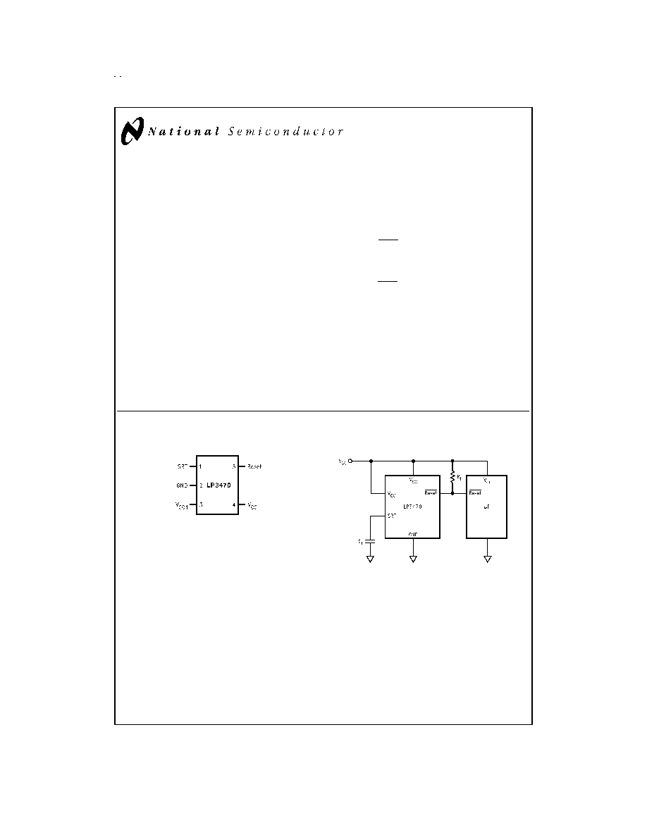
Pin Configuration and Basic Operating Circuit
Pin Configuration
DS100016-2
Top View
See NS Package Number
MA05B
Basic Operating Circuit
DS100016-1
June 1999
LP3470
T
iny
Power
On
Reset
Circuit
© 1999 National Semiconductor Corporation
DS100016
www.national.com
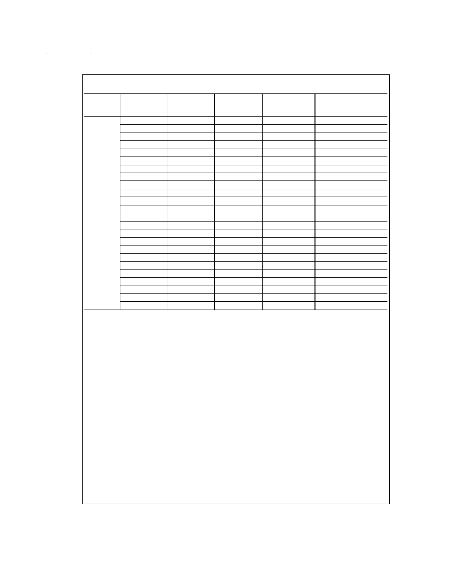
Ordering Information
Operating
Temperature
Range
Order
Number
Nominal
V
RTH
(V)
Package
Marking
Package
Type
Supplied As
-20∞C to
+85∞C
LP3470M5-2.63
2.63
D25B
SOT23-5
250 Units on Tape and Reel
LP3470M5X-2.63
2.63
D25B
SOT23-5
3k Units on Tape and Reel
LP3470M5-2.93
2.93
D26B
SOT23-5
250 Units on Tape and Reel
LP3470M5X-2.93
2.93
D26B
SOT23-5
3k Units on Tape and Reel
LP3470M5-3.08
3.08
D28B
SOT23-5
250 Units on Tape and Reel
LP3470M5X-3.08
3.08
D28B
SOT23-5
3k Units on Tape and Reel
LP3470M5-4.00
4.00
D29B
SOT23-5
250 Units on Tape and Reel
LP3470M5X-4.00
4.00
D29B
SOT23-5
3k Units on Tape and Reel
LP3470M5-4.38
4.38
D30B
SOT23-5
250 Units on Tape and Reel
LP3470M5X-4.38
4.38
D30B
SOT23-5
3k Units on Tape and Reel
LP3470M5-4.63
4.63
D31B
SOT23-5
250 Units on Tape and Reel
LP3470M5X-4.63
4.63
D31B
SOT23-5
3k Units on Tape and Reel
-40∞C to
+85∞C
LP3470IM5-2.63
2.63
D25C
SOT23-5
250 Units on Tape and Reel
LP3470IM5X-2.63
2.63
D25C
SOT23-5
3k Units on Tape and Reel
LP3470IM5-2.93
2.93
D26C
SOT23-5
250 Units on Tape and Reel
LP3470IM5X-2.93
2.93
D26C
SOT23-5
3k Units on Tape and Reel
LP3470IM5-3.08
3.08
D28C
SOT23-5
250 Units on Tape and Reel
LP3470IM5X-3.08
3.08
D28C
SOT23-5
3k Units on Tape and Reel
LP3470IM5-4.00
4.00
D29C
SOT23-5
250 Units on Tape and Reel
LP3470IM5X-4.00
4.00
D29C
SOT23-5
3k Units on Tape and Reel
LP3470IM5-4.38
4.38
D30C
SOT23-5
250 Units on Tape and Reel
LP3470IM5X-4.38
4.38
D30C
SOT23-5
3k Units on Tape and Reel
LP3470IM5-4.63
4.63
D31C
SOT23-5
250 Units on Tape and Reel
LP3470IM5X-4.63
4.63
D31C
SOT23-5
3k Units on Tape and Reel
www.national.com
2
Absolute Maximum Ratings
(Note 1)
If Military/Aerospace specified devices are required,
please contact the National Semiconductor Sales Office/
Distributors for availability and specifications.
V
CC
Voltage
-0.3V to +6V
Reset Voltage
-0.3V to +6V
Output Current (Reset)
10 mA
Operating Temperature Range
LP3470
-20∞C to +85∞C
LP3470I
-40∞C to +85∞C
Junction Temperature (T
Jmax
)
125∞C
Power Dissipation (T
A
= 25∞C) (Note
2)
300 mW
JA
(Note 2)
280∞C/W
Storage Temp. Range
-65∞C to +150∞C
Lead Temp. (Soldering, 5 sec)
260∞C
ESD Rating (Note 3)
2 kV
Electrical Characteristics
Limits in standard typeface are for T
J
= 25∞C, and limits in boldface type apply over the full operating temperature range, unless
otherwise specified. V
CC
= +2.4V to +5.0V unless otherwise noted.
Symbol
Parameter
Conditions
Typ (Note 4)
Min (Note 5)
Max (Note 5)
Units
V
CC
Operating Voltage Range
0.5
5.5
V
I
CC
V
CC
Supply Current
V
CC
= 4.5V
16
30
µA
V
RTH
Reset Threshold Voltage
(Note 6)
LP3470
V
RTH
0.99 V
RTH
0.99 V
RTH
1.01 V
RTH
1.01 V
RTH
V
LP3470I
V
RTH
0.99 V
RTH
0.985 V
RTH
1.01 V
RTH
1.015 V
RTH
V
HYST
Hysteresis Voltage (Note 7)
35
15
65
mV
t
PD
V
CC
to Reset Delay
V
CC
falling at 1 mV/µs
100
300
µs
t
RP
Reset Timeout Period (Note
8)
C
1
= 1 nF
2
1.0
3.5
ms
V
OL
Reset Output Voltage Low
V
CC
= 0.5V; I
OL
= 30 µA
0.1
V
V
CC
= 1.0V; I
OL
= 100 µA
0.1
V
CC
=V
RTH
-100 mV; I
OL
= 4
mA
0.4
R
1
External Pull-up Resistor
20
0.68
68
k
I
LEAK
Reset Output Leakage
Current
0.15
1
µA
6
Note 1: Absolute Maximum Ratings indicate limits beyond which damage to the device may occur. Electrical specifications do not apply when operating the device
beyond its operating conditions.
Note 2: The maximum power dissipation must be derated at elevated temperatures and is dictated by T
Jmax
(Maximum Junction Temperature),
JA
(Junction to Am-
bient Thermal Resistance), and T
A
(Ambient Temperature). The maximum allowable power dissipation at any temperature is P
Dmax
= (T
Jmax
- T
A
)/
JA
or the number
given in the Absolute Maximum Ratings, whichever is lower.
Note 3: The Human Body Model is a 100 pF capacitor discharged through a 1.5 k
resistor into each pin.
Note 4: Typical numbers are at 25∞C and represent the most likely parametric norm.
Note 5: Min. and Max. limits in standard typeface are 100% production tested at 25∞C. Min. and Max. limits in boldface are guaranteed through correlation using Sta-
tistical Quality Control (SQC) methods. The limits are used to calculate National's Average Outgoing Quality Level (AOQL).
Note 6: Factory-trimmed reset thresholds are available in 50 mV increments from 2.4V to 5.0V. Contact your National Semiconductor representative.
Note 7: V
HYST
affects the relation between V
CC
and Reset as shown in the timing diagram.
Note 8: t
RP
is programmable by varying the value of the external capacitor (C
1
) connected to pin SRT. The equation is: t
RP
= 2000 x C
1
(C
1
in µF and t
RP
in ms).
www.national.com
3
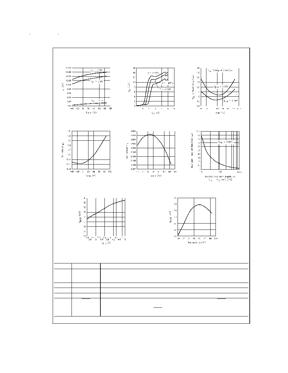
Typical Operating Characteristics
T
A
= +25∞C, unless otherwise specified.
Pin Description
Pin
Name
Function
1
SRT
Set Reset Time-out Input. Connect a capacitor between this input and ground to select the Reset
Time-out period (t
RP
). t
RP
= 2000 x C
1
(C
1
in µF and t
RP
in ms). If no capacitor is connected,
leave this pin floating.
2
GND
Ground pin.
3
V
CC1
Always connect to pin V
CC
(Pin 4).
4
V
CC
Supply voltage, and reset threshold monitor input.
5
Reset
Open-Drain, Active-Low reset output. Connect to an external pull-up resistor. Reset changes
from high to low whenever the monitored voltage (V
CC
) drops below the reset threshold voltage
(V
RTH
). Once V
CC
exceeds V
RTH
, Reset remains low for the reset timeout period (t
RP
) and then
goes high.
I
CC
vs Temperture
DS100016-10
I
CC
vs V
CC
DS100016-11
V
CC
to Reset Delay vs Temp
DS100016-13
Normalized t
RP
vs Temp.
DS100016-12
Normalized V
RTH
vs Temp.
DS100016-8
Transient Rejection
DS100016-6
V
HYST
vs V
RTH
DS100016-14
V
HYST
vs Temperature
DS100016-9
www.national.com
4

Functional Block Diagram
Application Information
Reset Timeout Period
The Reset Timeout Period (t
RP
) is programmable using an
external capacitor (C
1
) connected to pin SRT of LP3470. A
Ceramic chip capacitor rated at or above 10V is sufficient.
The Reset Timeout Period (t
RP
) can be calculated using the
following formula:
t
RP
(ms) = 2000 x C
1
(µF).
For example a C
1
of 100 nF will achieve a t
RP
of 200 ms. If
no delay due to t
RP
is needed in a certain application, the pin
SRT should be left floating.
Reset Output
In applications like microprocessor (µP) systems, errors
might
occur
in
system
operation
during
power-up,
power-down, or brownout conditions. It is imperative to
monitor the power supply voltage in order to prevent these
errors from occurring.
The LP3470 asserts a reset signal whenever the V
CC
supply
voltage is below a threshold (V
RTH
) voltage. Reset is guaran-
teed to be a logic low for V
CC
>
0.5V. Once V
CC
exceeds the
reset threshold, the reset is kept asserted for a time period
(t
RP
) programmed by an external capacitor (C
1
); after this in-
terval Reset goes to logic high. If a brownout condition oc-
curs (monitored voltage falls below the reset threshold minus
a small hysteresis), Reset goes low. When V
CC
returns
above the reset threshold, Reset remains low for a time pe-
riod t
RP
before going to logic high.
Pull-up Resistor Selection
The LP3470's Reset output structure is a simple open-drain
N-channel MOSFET switch. A pull-up resistor (R
1
) should be
connected to V
CC
.
R
1
should be large enough to limit the current through the
output MOSFET (Q
1
) below 10 mA. A resistor value of more
than 680
guarantees this. R
1
should also be small enough
to ensure a logic high while supplying all the leakage current
through the Reset pin. A resistor value of less than 68k
sat-
isfies this condition. A typical pull-up resistor value of 20 k
is sufficient in most applications.
Negative-Going V
CC
Transients
The
LP3470
is
relatively
immune
to
short
duration
negative-going V
CC
transients (glitches). The Typical Oper-
ating Characteristics show the Maximum Transient Duration
vs. Negative Transient Amplitude (graph titled Transient Re-
jection), for which reset pulses are not generated. This graph
shows the maximum pulse width a negative-going V
CC
tran-
sient may typically have without causing a reset pulse to be
issued. As the transient amplitude increases (i.e. goes far-
ther below the reset threshold), the maximum allowable
pulse width decreases. A 0.1 µF bypass capacitor mounted
close to V
CC
provides additional transient immunity.
DS100016-3
www.national.com
5