 | –≠–ª–µ–∫—Ç—Ä–æ–Ω–Ω—ã–π –∫–æ–º–ø–æ–Ω–µ–Ω—Ç: LP365N | –°–∫–∞—á–∞—Ç—å:  PDF PDF  ZIP ZIP |
TL H 5023
LP265LP365
Micropower
Programmable
Quad
Comparator
December 1994
LP265 LP365 Micropower Programmable
Quad Comparator
General Description
The LP365 consists of four independent voltage compara-
tors The comparators can be programmed four at the
same time for various supply currents input currents re-
sponse times and output current drives This is accom-
plished by connecting a single resistor between the V
CC
and I
SET
pins
These comparators can be operated from split power sup-
plies or from a single power supply over a wide range of
voltages The input can sense signals at ground level even
with single supply operation The unique output NPN tran-
sistor stages are uncommitted to either power supply They
can be connected directly to various logic system supplies
so that they are highly flexible to interface with various logic
families
Application areas include battery power circuits threshold
detectors zero crossing detectors simple serial A D con-
verters VCO multivibrators voltage converters power se-
quencers and high performance V F converters and RTD
linearization
Features
Y
Single programming resistor to tailor power consump-
tion
input current
speed and output current drive
capability
Y
Wide single supply voltage range or dual supplies (4
V
DC
to 36 V
DC
or
g
2 0 V
DC
to
g
18 V
DC
)
Y
Low supply current drain (10 mA) and low power
consumption (10 mW comparator)
I
SET
e
0 5 mA
V
CC
e
5
VDC
Y
Uncommitted output stage
selectable output levels
Y
Output directly compatible with DTL TTL CMOS MOS
or other special logic families
Y
Input common-mode range includes ground
Y
Differential input voltage equal to the power supply
voltage
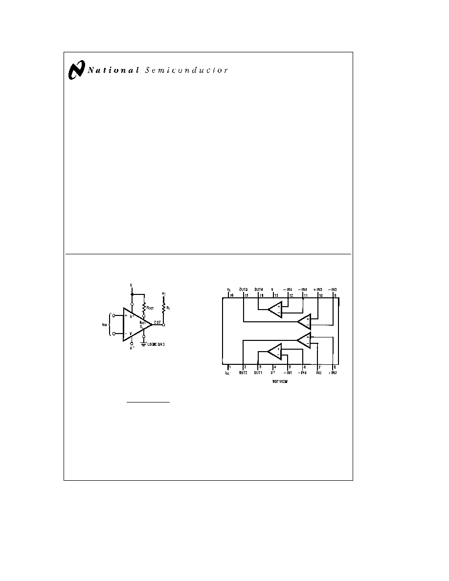
Typical Connection
TL H 5023 ≠ 1
Programming Equation
I
SET
e
(V
a
)
b
(V
b
)
b
1 3V
R
SET
I
SUPPLY
22
c
I
SET
Connection Diagram
Dual-In-Line Package
TL H 5023 ≠ 2
Order Number LP365M LP365AN or LP365N
See NS Package Numbers M16A or N16A
C1995 National Semiconductor Corporation
RRD-B30M115 Printed in U S A
Absolute Maximum Ratings
If Military Aerospace specified devices are required
please contact the National Semiconductor Sales
Office Distributors for availability and specifications
Supply Voltage
36 V
DC
or
g
18 V
DC
Differential Input Voltage
g
36 V
DC
Input Voltage (Note 1)
b
0 3V to
a
36 V
DC
Output Short Circuit to V
E
(Note 2)
Continuous
V
OUT
with Respect to V
E
V
E
b
7V
s
V
OUT
s
V
E
a
36V
ESD Tolerance (Note 10)
2000V
M Package
N Package
Power Dissipation (Note 3)
500 mW
500 mW
T
j
Max
115 C
115 C
i
jA
115 C W
90 C W
Lead Temp
(Soldering
10 sec )
260 C
(Vapor Phase
60 sec )
215 C
(Infrared
15 sec )
220 C
Operating Temp Range LP365
0 C
s
T
A
s
a
70 C
Storage Temp Range
b
40 C
s
T
A
s
a
150 C
Electrical Characteristics
(Note 4) Low power V
S
e
5V I
SET
e
10 mA
LP365A
LP365
Symbol
Parameter
Conditions
Tested
Design
Tested
Design
Units
Typ
Limit
Limit
Typ
Limit
Limit
(Limit)
(Note 5)
(Note 6)
(Note 5)
(Note 6)
V
OS
Input Offset
V
CM
e
OV
1
3
6
3
6
9
mV
Voltage
R
S
e
100
(Max)
I
OS
Input Offset
V
CM
e
0V
2
20
50
4
25
75
nA
Current
LP265
4
25
150
(Max)
I
B
Input Bias
V
CM
e
0V
10
50
125
15
75
200
nA
Current
LP265
15
75
300
(Max)
A
VOL
Large Signal
R
L
e
100k
500
50
50
300
25
25
V mV
Voltage Gain
(Min)
V
CM
Input Common-
0
0
0
0
V
Mode Voltage
(Max)
Range
3
3
3
3
V
(Min)
CMRR
Common-Mode
0
s
V
CM
s
3V
85
75
70
80
75
70
dB
Rejection Ratio
(Min)
PSRR
Supply Voltage
g
2 5V
s
V
S
75
65
65
70
65
65
dB
Rejection Ratio
s g
3 5V
(Min)
I
S
Supply Current
All Inputs
e
0V
215
250
300
225
275
300
m
A
R
L
e
%
(Max)
V
OH
Output Voltage
V
C
e
5V
V
High
V
E
e
0V
4 9
4 5
4 9
4 5
(Min)
R
L
e
100k
V
OL
Output Voltage
V
E
e
0V
0 4
0 4
0 4
0 4
V
Low
(Max)
I
SINK
Output Sink
V
E
e
0V
2 4
1 2
0 6
2 0
0 8
0 4
mA
Current
V
O
e
0 4V
(Min)
I
LEAK
Output Leakage
V
C
e
5V
2
50
5000
2
100
5000
nA
Current
V
E
e
0V
(Max)
t
R
Response Time
V
CC
e
5V
V
E
e
0V
R
L
e
5k
4
4
m
s
C
L
e
10 pF
(Note 7)
2
Electrical Characteristics
(Continued) (Note 8) High power V
S
e
g
15V I
SET
e
100 mA
LP365A
LP365
Symbol
Parameter
Conditions
Tested
Design
Tested
Design
Units
Typ
Limit
Limit
Typ
Limit
Limit
(Limit)
(Note 5)
(Note 6)
(Note 5)
(Note 6)
V
OS
Input Offset
V
CM
e
0V
1
3
6
3
6
9
mV
Voltage
R
S
e
100
(Max)
I
OS
Input Offset
V
CM
e
0V
5
50
100
10
90
200
nA
Current
LP265
10
90
500
(Max)
I
B
Input Bias
V
CM
e
0V
60
200
500
80
300
500
nA
Current
LP265
80
300
800
(Max)
A
VOL
Large Signal
R
L
e
15k
500
100
100
500
100
100
V mV
Voltage Gain
(Min)
V
CM
Input Common-
b
15
b
15
b
15
b
15
V
Mode Voltage
(Max)
Range
13
13
13
13
V
(Min)
CMRR
Common-Mode
b
15V
s
V
CM
85
75
70
80
75
70
dB
Rejection Ratio
s
13V
(Min)
PSRR
Supply Voltage
g
10V
s
V
S
80
70
70
75
70
70
dB
Rejection Ratio
s g
15V
(Min)
I
S
Supply Current
All Inputs
e
0V
2 6
3
3 3
2 8
3 5
3 7
mA
R
L
e
%
LP265
2 8
3 5
4 3
(Max)
V
OH
Output Voltage
V
C
e
5V
V
High
V
E
e
0V
4 9
4 5
4 9
4 5
(Min)
R
L
e
100k
V
OL
Output Voltage
V
E
e
0V
0 4
0 4
0 4
0 4
V
Low
(Max)
I
SINK
Output Sink
V
E
e
0V
10
8
5 5
7 5
6
4
mA
Current
V
O
e
0 4V
(Min)
I
LEAK
Output Leakage
V
C
e
15V
5
50
5000
5
50
5000
nA
Current
V
E
e b
15V
(Max)
t
R
Response Time
V
CC
e
5V
V
E
e
0V
R
L
e
5k
1 0
1 0
m
s
C
L
e
10 pF
(Note 7)
Note 1
The input voltage is not allowed to go 0 3V above V
a
or
b
0 3V below V
b
as this will turn on a parasitic transistor causing large currents to flow through
the device
Note 2
Short circuits from the output to V
a
may cause excessive heating and eventual destruction The current in the output leads and the V
E
lead should not be
allowed to exceed 30 mA The output should not be shorted to V
b
if V
E
s
(V
b
)
a
7V
Note 3
For operating at elevated temperatures these devices must be derated based on a thermal resistance of i
jA
and T
j
max T
j
e
T
A
a
i
jA
P
D
Note 4 Boldface numbers apply at temperature extremes
All other numbers apply at T
A
e
T
j
e
25 C V
a
e
5V V
b
e
0V I
SET
e
10 mA R
L
e
100k and
V
C
e
5V as shown in the Typical Connection diagram
Note 5
Guaranteed and 100% production tested
Note 6
Guaranteed (but not 100% production tested) over the operating temperature and supply voltage ranges These limits are not used to calculate out-going
quality levels
Note 7
The response time specified is for a 100 mV input step with 5 mV overdrive
Note 8 Boldface numbers apply at temperature extremes
All other numbers apply at T
A
e
T
j
e
25 C V
a
e a
15V V
b
e b
15V I
SET
e
100 mA R
L
e
100k and
V
C
e
5V as shown in the Typical Connection diagram
Note 9
See AN-450 ``Surface Mounting Methods and Their Effect on Product Reliability'' for other methods of soldering surface mount devices
Note 10
Human body model 1 5 kX in series with 100 pF
3
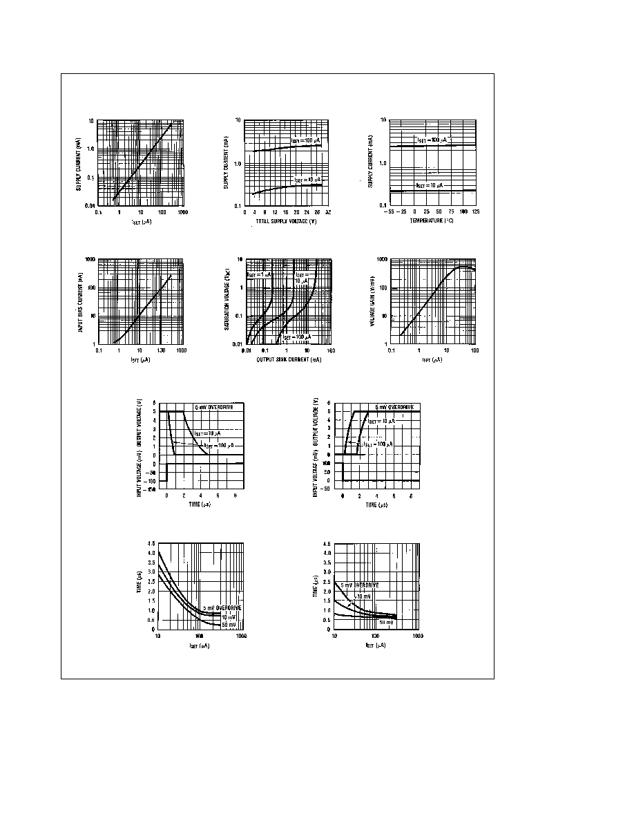
Typical Performance Characteristics
Supply Current vs I
SET
Supply Current vs Supply
Voltage
Supply Current vs
Temperature
Input Bias Current vs I
SET
Output Saturation Voltage
Voltage Gain vs I
SET
Response Time
Negative Transition
Response Time
Positive Transition
Response Time
Negative Transition
Response Time
Positive Transition
TL H 5023 ≠ 3
4
Typical Applications
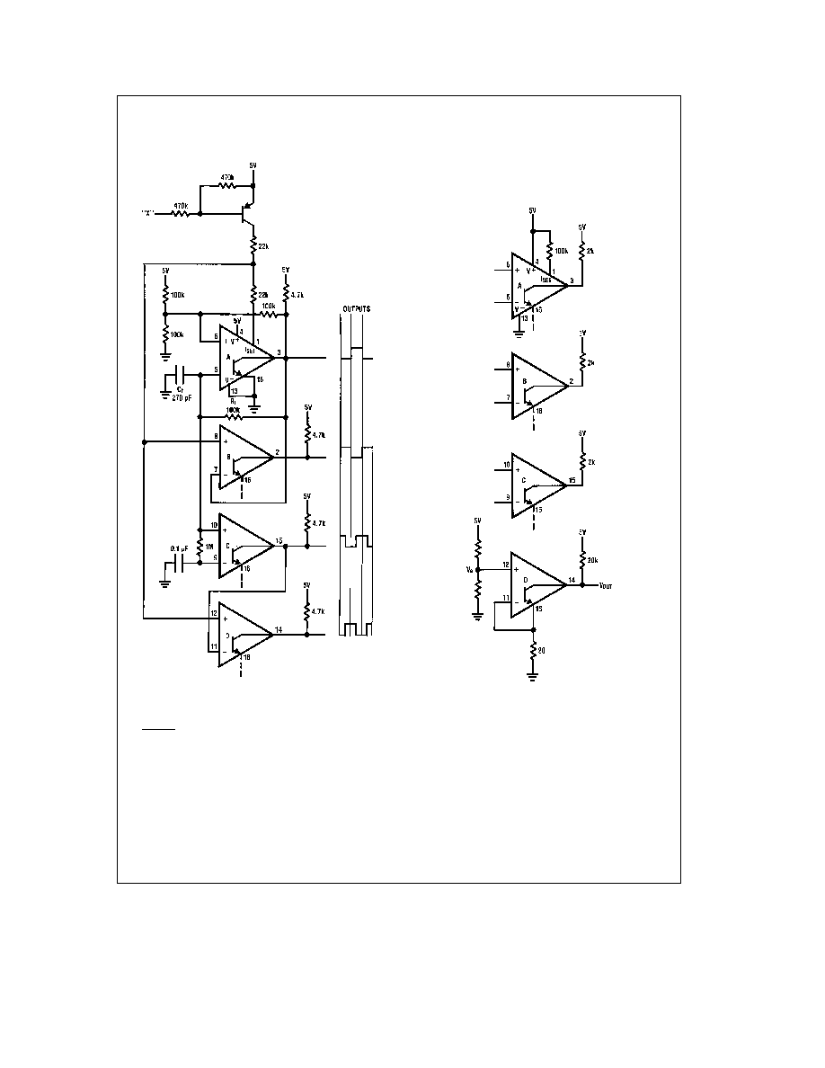
Gated 4-Phase Oscillator
TL H 5023 ≠ 4
f
e
20 kHz
f
e
1
1 6
R
t
C
t
All four phases run when X is low When X is high oscillation stops and
power drain is zero
``Voting'' Comparator
TL H 5023 ≠ 5
If V
E
e
0 25V then V
OUT
will be low if 1 of the 3 other outputs are low
Choice of V
E
e
0 50V causes V
OUT
to be low if 2 of the 3 other outputs are
low V
E
e
0 75V will cause V
OUT
to be low if all 3 other outputs are low
5