LP3875-ADJ
1.5A Fast Ultra Low Dropout Linear Regulators
General Description
The LP3875-ADJ fast ultra low-dropout linear regulators op-
erate from a +2.5V to +7.0V input supply. These ultra low
dropout linear regulators respond very quickly to step
changes in load, which makes them suitable for low voltage
microprocessor applications. The LP3875-ADJ is developed
on a CMOS process which allows low quiescent current
operation independent of output load current. This CMOS
process also allows the LP3875-ADJ to operate under ex-
tremely low dropout conditions.
Dropout Voltage: Ultra low dropout voltage; typically 38mV
at 150mA load current and 380mV at 1.5A load current.
Ground Pin Current: Typically 6mA at 1.5A load current.
Shutdown Mode: Typically 10nA quiescent current when
the shutdown pin is pulled low.
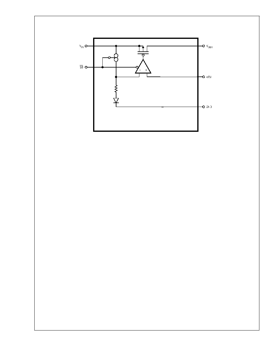
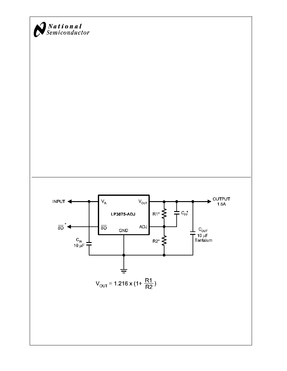
Adjustable Output Voltage: The output voltage may be
programmed via two external resistors.
Features
n
Ultra low dropout voltage
n
Low ground pin current
n
Load regulation of 0.06%
n
10nA quiescent current in shutdown mode
n
Guaranteed output current of 1.5A DC
n
Available in TO-263, TO-220 and SOT-223 packages
n
Minimum output capacitor requirements
n
Overtemperature/overcurrent protection
n
-40∞C to +125∞C junction temperature range
Applications
n
Microprocessor power supplies
n
GTL, GTL+, BTL, and SSTL bus terminators
n
Power supplies for DSPs
n
SCSI terminator
n
Post regulators
n
High efficiency linear regulators
n
Battery chargers
n
Other battery powered applications
Typical Application Circuit
20074645
*See Application Hints
July 2005
LP3875-ADJ
1.5A
Fast
Ultra
Low
Dropout
Linear
Regulators
© 2005 National Semiconductor Corporation
DS200746
www.national.com
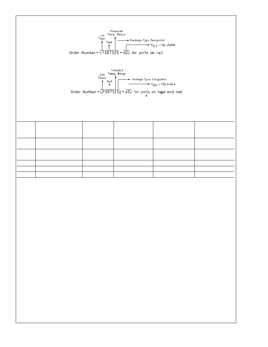
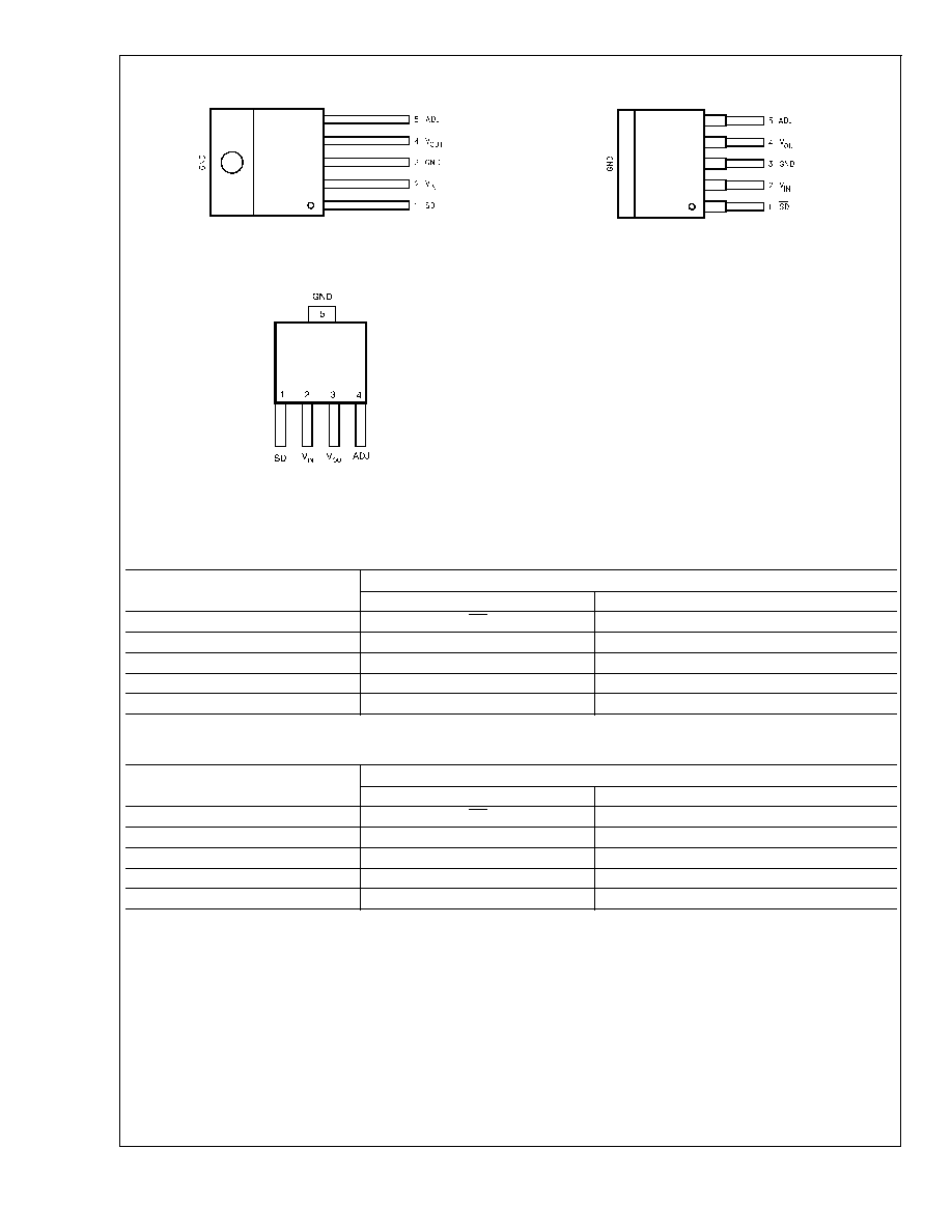
Ordering Information
20074631
Package Type Designator is "T" for TO220 package, "S" for TO263 package, and "MP" for SOT-223 package.
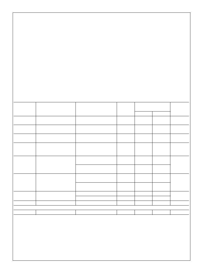
TABLE 1. Package Marking and Ordering Information
Output
Voltage
Order Number
Description
(Current,
Option)
Package Type
Package Marking
Supplied As:
ADJ
LP3875EMP-ADJ
1.5A, Adj
SOT223-5
LHSB
1000 Units on Tape
and Reel
ADJ
LP3875EMPX-ADJ
1.5A, Adj
SOT223-5
LHSB
2000 Units on Tape
and Reel
ADJ
LP3875ES-ADJ
1.5A, Adj
TO263-5
LP3875ES-ADJ
Rail
ADJ
LP3875ESX-ADJ
1.5A, Adj
TO263-5
LP3875ES-ADJ
Tape and Reel
ADJ
LP3875ET-ADJ
1.5A, Adj
TO220-5
LP3875ET-ADJ
Rail
LP3875-ADJ
www.national.com
3
Absolute Maximum Ratings
(Note 1)
If Military/Aerospace specified devices are required,
please contact the National Semiconductor Sales Office/
Distributors for availability and specifications.
Storage Temperature Range
-65∞C to +150∞C
Lead Temperature
(Soldering, 5 sec.)
260∞C
ESD Rating (Note 3)
2 kV
Power Dissipation (Note 2)
Internally Limited
Input Supply Voltage (Survival)
-0.3V to +7.5V
Shutdown Input Voltage
(Survival)
-0.3V to +7.5V
Output Voltage (Survival), (Note
6), (Note 7)
-0.3V to +6.0V
I
OUT
(Survival)
Short Circuit Protected
Operating Ratings
Input Supply Voltage (Operating),
(Note 10)
2.5V to 7.0V
Shutdown Input Voltage
(Operating)
-0.3V to 7.0V
Maximum Operating Current (DC)
1.5A
Operating Junction Temp. Range
-40∞C to +125∞C
Electrical Characteristics
LP3875-ADJ
Limits in standard typeface are for T
J
= 25∞C, and limits in boldface type apply over the full operating temperature range.
Unless otherwise specified: V
IN
= V
O(NOM)
+ 1V, I
L
= 10 mA, C
OUT
= 10µF, V
SD
= 2V.
Symbol
Parameter
Conditions
Typ
(Note 4)
LP3875-ADJ
(Note 5)
Units
Min
Max
V
ADJ
Adjust Pin Voltage
V
OUT
+1V
V
IN
7V
10 mA
I
L
1.5A
1.216
1.198
1.180
1.234
1.253
V
I
ADJ
Adjust Pin Input Current
V
OUT
+1V
V
IN
7V
10 mA
I
L
1.5A
10
100
nA
V
OL
Output Voltage Line
Regulation (Note 8)
V
OUT
+1V
V
IN
7.0V
0.02
0.06
%
V
O
/
I
OUT
Output Voltage Load
Regulation
(Note 8)
10 mA
I
L
1.5A
0.06
0.12
%
V
IN
- V
OUT
Dropout Voltage
(Note 9)
I
L
= 150 mA
38
50
60
mV
I
L
= 1.5A
380
450
550
I
GND
Ground Pin Current In
Normal Operation Mode
I
L
= 150 mA
5
9
10
mA
I
L
= 1.5A
6
14
15
I
GND
Ground Pin Current In
Shutdown Mode
V
SD
0.3V
0.01
10
µA
-40∞C
T
J
85∞C
50
I
O(PK)
Peak Output Current
V
O
V
O(NOM)
- 4%
1.8
A
Short Circuit Protection
I
SC
Short Circuit Current
3.2
A
LP3875-ADJ
www.national.com
5