LP3876-ADJ
3A Fast Ultra Low Dropout Linear Regulator
General Description
The LP3876-ADJ fast ultra low-dropout linear regulators op-
erate from a +2.5V to +7.0V input supply. These ultra low
dropout linear regulators respond very quickly to step
changes in load, which makes them suitable for low voltage
microprocessor applications. The LP3876-ADJ is developed
on a CMOS process which allows low quiescent current
operation independent of output load current. This CMOS
process also allows the LP3876-ADJ to operate under ex-
tremely low dropout conditions.
Dropout Voltage: Ultra low dropout voltage; typically 80mV
at 300mA load current and 800mV at 3A load current.
Ground Pin Current: Typically 6mA at 3A load current.
Shutdown Mode: Typically 1µA quiescent current when the
shutdown pin is pulled low.
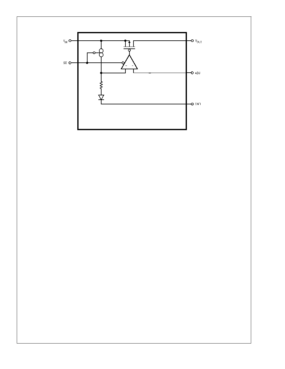
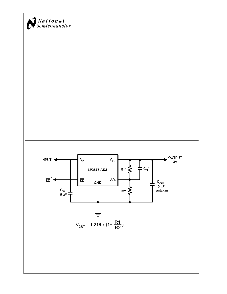
Adjustable Output Voltage: The output voltage may be
programmed via two external resistors.
Features
n
Ultra low dropout voltage
n
Low ground pin current
n
Load regulation of 0.08%
n
1µA quiescent current in shutdown mode
n
Guaranteed output current of 3A DC
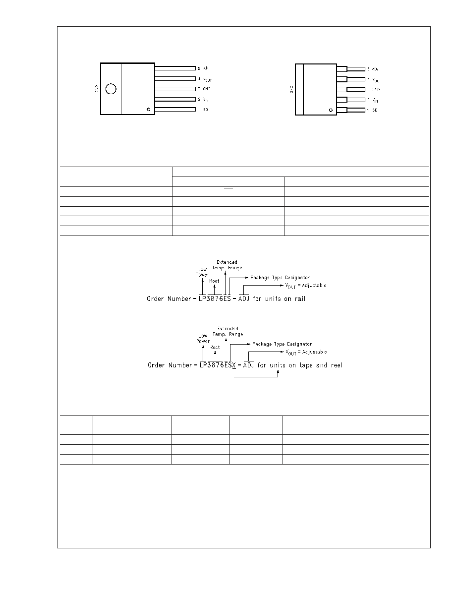
n
Available in TO-263 and TO-220 packages
n
Minimum output capacitor requirements
n
Overtemperature/overcurrent protection
n
-40∞C to +125∞C junction temperature range
Applications
n
Microprocessor power supplies
n
GTL, GTL+, BTL, and SSTL bus terminators
n
Power supplies for DSPs
n
SCSI terminator
n
Post regulators
n
High efficiency linear regulators
n
Battery chargers
n
Other battery powered applications
Typical Application Circuit
20074445
*See Application Hints
September 2003
LP3876-ADJ
3A
Fast
Ultra
Low
Dropout
Linear
Regulator
© 2003 National Semiconductor Corporation
DS200744
www.national.com
Absolute Maximum Ratings
(Note 1)
If Military/Aerospace specified devices are required,
please contact the National Semiconductor Sales Office/
Distributors for availability and specifications.
Storage Temperature Range
-65∞C to +150∞C
Lead Temperature
(Soldering, 5 sec.)
260∞C
ESD Rating (Note 3)
2 kV
Power Dissipation (Note 2)
Internally Limited
Input Supply Voltage (Survival)
-0.3V to +7.5V
Shutdown Input Voltage
(Survival)
-0.3V to 7.5V
Output Voltage (Survival), (Note
6), (Note 7)
-0.3V to +6.0V
I
OUT
(Survival)
Short Circuit Protected
Operating Ratings
Input Supply Voltage (Operating),
(Note 10)
2.5V to 7.0V
Shutdown Input Voltage
(Operating)
-0.3V to 7.0V
Maximum Operating Current (DC)
3A
Operating Junction Temp. Range
-40∞C to +125∞C
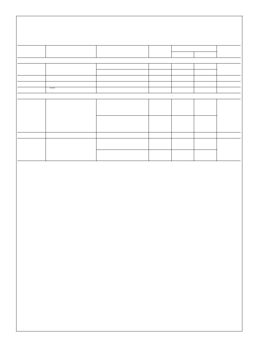
Electrical Characteristics
LP3876-ADJ
Limits in standard typeface are for T
J
= 25∞C, and limits in boldface type apply over the full operating temperature range.
Unless otherwise specified: V
IN
= V
O(NOM)
+ 1.5V, I
L
= 10 mA, C
OUT
= 10µF, V
SD
= 2V.
Symbol
Parameter
Conditions
Typ
(Note 4)
LP3876-ADJ (Note 5)
Units
Min
Max
V
ADJ
Adjust Pin Voltage
V
OUT
+1.5V
V
IN
7V
10 mA
I
L
3A
1.216
1.198
1.180
1.234
1.253
V
I
ADJ
Adjust Pin Input Current
V
OUT
+1.5V
V
IN
7V
10 mA
I
L
3A
10
100
nA
V
OL
Output Voltage Line
Regulation (Note 8)
V
OUT
+1.5V
V
IN
7.0V
0.02
0.06
%
V
O
/
I
OUT
Output Voltage Load
Regulation
(Note 8)
10 mA
I
L
3A
0.08
0.14
%
V
IN
- V
OUT
Dropout Voltage
(Note 9)
I
L
= 300 mA
80
105
125
mV
I
L
= 3A
800
1000
1200
I
GND
Ground Pin Current In
Normal Operation Mode
I
L
= 300 mA
5
9
10
mA
I
L
= 3A
6
14
15
I
GND
Ground Pin Current In
Shutdown Mode
V
SD
0.3V
1
10
µA
-40∞C
T
J
85∞C
50
I
O(PK)
Peak Output Current
V
O
V
O(NOM)
- 4%
4.5
A
SHORT CIRCUIT PROTECTION
I
SC
Short Circuit Current
6
A
LP3876-ADJ
www.national.com
4
Electrical Characteristics
LP3876-ADJ
(Continued)
Limits in standard typeface are for T
J
= 25∞C, and limits in boldface type apply over the full operating temperature range.
Unless otherwise specified: V
IN
= V
O(NOM)
+ 1.5V, I
L
= 10 mA, C
OUT
= 10µF, V
SD
= 2V.
Symbol
Parameter
Conditions
Typ
(Note 4)
LP3876-ADJ (Note 5)
Units
Min
Max
SHUTDOWN INPUT
V
SDT
Shutdown Threshold
Output = High
V
IN
2
V
Output = Low
0
0.3
T
dOFF
Turn-off delay
I
L
= 3A
20
µs
T
dON
Turn-on delay
I
L
= 3A
25
µs
I
SD
SD Input Current
V
SD
= V
IN
1
nA
AC PARAMETERS
PSRR
Ripple Rejection
V
IN
= V
OUT
+ 1V
C
OUT
= 10uF
V
OUT
= 3.3V, f = 120Hz
73
dB
V
IN
= V
OUT
+ 0.5V
C
OUT
= 10uF
V
OUT
= 3.3V, f = 120Hz
57
n(l/f
Output Noise Density
f = 120Hz
0.8
µV
e
n
Output Noise Voltage
BW = 10Hz ≠ 100kHz
V
OUT
= 2.5V
150
µV (rms)
BW = 300Hz ≠ 300kHz
V
OUT
= 2.5V
100
Note 1: Absolute maximum ratings indicate limits beyond which damage to the device may occur. Operating ratings indicate conditions for which the device is
intended to be functional, but does not guarantee specific performance limits. For guaranteed specifications and test conditions, see Electrical Characteristics. The
guaranteed specifications apply only for the test conditions listed. Some performance characteristics may degrade when the device is not operated under the listed
test conditions.
Note 2: At elevated temperatures, devices must be derated based on package thermal resistance. The devices in TO220 package must be derated at
jA
= 50∞C/W
(with 0.5in
2
, 1oz. copper area), junction-to-ambient (with no heat sink). The devices in the TO263 surface-mount package must be derated at
jA
= 60∞C/W (with
0.5in
2
, 1oz. copper area), junction-to-ambient. See Application Hints.
Note 3: The human body model is a 100pF capacitor discharged through a 1.5k
resistor into each pin.
Note 4: Typical numbers are at 25∞C and represent the most likely parametric norm.
Note 5: Limits are guaranteed by testing, design, or statistical correlation.
Note 6: If used in a dual-supply system where the regulator load is returned to a negative supply, the output must be diode-clamped to ground.
Note 7: The output PMOS structure contains a diode between the V
IN
and V
OUT
terminals. This diode is normally reverse biased. This diode will get forward biased
if the voltage at the output terminal is forced to be higher than the voltage at the input terminal. This diode can typically withstand 200mA of DC current and 1Amp
of peak current.
Note 8: Output voltage line regulation is defined as the change in output voltage from the nominal value due to change in the input line voltage. Output voltage load
regulation is defined as the change in output voltage from the nominal value due to change in load current.
Note 9: Dropout voltage is defined as the minimum input to output differential voltage at which the output drops 2% below the nominal value. Dropout voltage
specification applies only to output voltages of 2.5V and above. For output voltages below 2.5V, the drop-out voltage is nothing but the input to output differential,
since the minimum input voltage is 2.5V.
Note 10: The minimum operating value for V
IN
is equal to either [V
OUT(NOM)
+ V
DROPOUT
] or 2.5V, whichever is greater.
LP3876-ADJ
www.national.com
5