LP3878-ADJ
Micropower 800mA Low Noise "Ceramic Stable"
Adjustable Voltage Regulator for 1V to 5V Applications
General Description
The LP3878-ADJ is an 800 mA adjustable output voltage
regulator designed to provide high performance and low
noise in applications requiring output voltages as low as
1.0V.
Using an optimized VIP
TM
(Vertically Integrated PNP) pro-
cess, the LP3878-ADJ delivers superior performance:
Ground Pin Current: Typically 5.5 mA
@
800 mA load, and
180 µA
@
100 µA load.
Low Power Shutdown: The LP3878-ADJ draws less than
10 µA quiescent current when shutdown pin is pulled low.
Precision Output: Guaranteed output voltage accuracy is
1% at room temperature.
Low Noise: Broadband output noise is only 18 µV (typical)
with 10 nF bypass capacitor.
Features
n
1.0V to 5.5V output
n
Designed for use with low ESR ceramic capacitors
n
Very low output noise
n
8 Lead PSOP and LLP surface mount package
n
<
10 µA quiescent current in shutdown
n
Low ground pin current at all loads
n
Over-temperature/over-current protection
n
-40∞C to +125∞C operating junction temperature range
Applications
n
ASIC Power Supplies In:
- Desktops, Notebooks and Graphic Cards
- Set Top Boxes, Printers and Copiers
n
DSP and FPGA Power Supplies
n
SMPS Post-Regulator
n
Medical Instrumentation
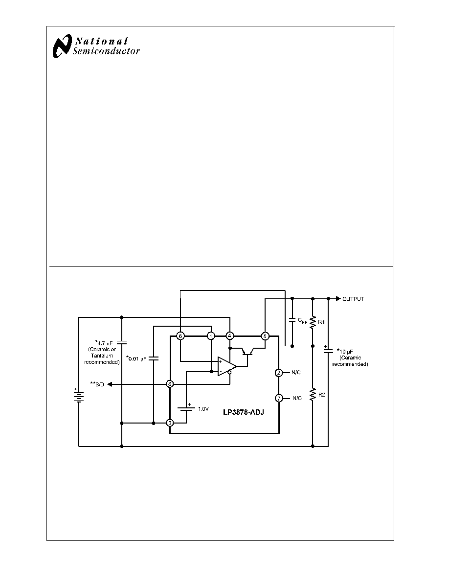
Basic Application Circuit
20120903
*Capacitance values shown are minimum required to assure stability. Larger output capacitor provides improved dynamic response. Output capacitor must
meet ESR requirements (see Application Information).
**The Shutdown pin must be actively terminated (see Application Information). Tie to INPUT (Pin 4) if not used.
VIP
TM
is a trademark of National Semiconductor Corporation.
May 2005
LP3878-ADJ
Micropower
800mA
Low
Noise
"Ceramic
Stable"
Adjustable
V
oltage
Regulator
for
1V
to
5V
Applications
© 2005 National Semiconductor Corporation
DS201209
www.national.com
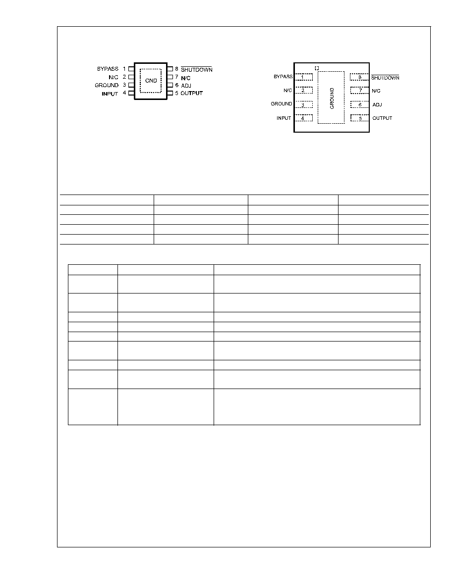
Connection Diagrams
8 Lead PSOP Package (MRA)
8 Lead LLP Surface Mount Package (SD)
20120930
Top View
See NS Package Number MRA08A
20120950
Top View
See NS Package Number SDC08A
Ordering Information
TABLE 1. Package Marking and Ordering Information
Output Voltage
Grade
Order Information
Supplied as:
ADJ
STD
LP3878MR-ADJ
95 Units per Rail
ADJ
STD
LP3878MRX-ADJ
2500 Units on Tape and Reel
ADJ
STD
LP3878SD-ADJ
1000 Units on Tape and Reel
ADJ
STD
LP3878SDX-ADJ
4500 Units on Tape and Reel
Pin Description
PIN
NAME
FUNCTION
1
BYPASS
The capacitor connected between BYPASS and GROUND lowers
output noise voltage level and is required for loop stability.
2
N/C
DO NOT CONNECT. This pin is used for post package test and must
be left floating.
3
GROUND
Device ground.
4
INPUT
Input source voltage.
5
OUTPUT
Regulated output voltage.
6
ADJ
Provides feedback to error amplifier from the resistive divider that sets
the output voltage.
7
N/C
No internal connection.
8
SHUTDOWN
Output is enabled above turn-on threshold voltage. Pull down to turn off
regulator output.
PSOP, LLP
DAP
SUBSTRATE
GROUND
The exposed die attach pad should be connected to a thermal pad at
ground potential. For additional information on using National
Semiconductor's Non Pull Back LLP package, please refer to LLP
application note AN-1187
LP3878-ADJ
www.national.com
2
Absolute Maximum Ratings
(Note 1)
If Military/Aerospace specified devices are required,
please contact the National Semiconductor Sales Office/
Distributors for availability and specifications.
Storage Temperature Range
-65∞C to +150∞C
Operating Junction
Temperature
Range
-40∞C to +125∞C
Lead Temperature
(Soldering, 5
seconds)
260∞C
ESD Rating (Note 2)
2 kV
Shutdown Pin
1kV
Power Dissipation (Note 3)
Internally Limited
Input Supply Voltage (Survival)
-0.3V to +16V
Input Supply Voltage (Typical
Operating)
2.5V to +16V
ADJ Pin
-0.3V to +6V
Output Voltage (Survival) (Note 4)
-0.3V to +6V
I
OUT
(Survival)
Short Circuit
Protected
Input-Output Voltage (Survival)
(Note 5)
-0.3V to +16V
Electrical Characteristics
Limits in standard typeface are for T
J
= 25∞C, and limits in boldface type apply over the temperature range of -40∞C to 125∞C.
Limits are guaranteed through design, testing, or correlation. The limits are used to calculate National's Average Outgoing
Quality Level (AOQL). Unless otherwise specified: V
IN
= 3.0V, V
OUT
= 1V, I
L
= 1 mA, C
OUT
= 10 µF, C
IN
= 4.7 µF, V
S/D
= 2V,
C
BYPASS
= 10 nF.
Symbol
Parameter
Conditions
Min
Typical
Max
Units
V
ADJ
Adjust Pin Voltage
0.99
1.00
1.01
V
1 mA
I
L
800 mA
3.0V
V
IN
6V
0.98
0.97
1.00
1.02
1.03
Output Voltage Line
Regulation
3.0V
V
IN
16V
0.007
0.014
%/V
0.032
V
IN
(min)
Minimum Input
Voltage Required
To Maintain Output
Regulation
I
L
= 800 mA
V
OUT
V
OUT(NOM)
- 1%
2.5
3.1
V
I
L
= 800 mA
V
OUT
V
OUT(NOM)
- 1%
0
T
J
125∞C
2.5
2.8
I
L
= 750 mA
V
OUT
V
OUT(NOM)
- 1%
2.5
3.0
V
DO
Dropout Voltage
(Note 6)
V
OUT
= 3.8V
I
L
= 100 µA
1
2
3
mV
I
L
= 200 mA
150
200
300
I
L
= 800 mA
475
600
1100
I
GND
Ground Pin Current
I
L
= 100 µA
180
200
µA
225
I
L
= 200 mA
1.5
2
mA
3.5
I
L
= 800 mA
5.5
8.5
15
I
O
(PK)
Peak Output
Current
V
OUT
V
OUT(NOM)
- 5%
1200
mA
I
O
(MAX)
Short Circuit
Current
R
L
= 0 (Steady State)
1300
e
n
Output Noise
Voltage (RMS)
BW = 100 Hz to 100 kHz
C
BYPASS
= 10 nF
18
µV(RMS)
Ripple Rejection
f = 1 kHz
60
dB
I
ADJ
ADJ Pin Bias
Current (Sourcing)
I
L
= 800 mA
200
nA
LP3878-ADJ
www.national.com
3
Electrical Characteristics
(Continued)
Limits in standard typeface are for T
J
= 25∞C, and limits in boldface type apply over the temperature range of -40∞C to 125∞C.
Limits are guaranteed through design, testing, or correlation. The limits are used to calculate National's Average Outgoing
Quality Level (AOQL). Unless otherwise specified: V
IN
= 3.0V, V
OUT
= 1V, I
L
= 1 mA, C
OUT
= 10 µF, C
IN
= 4.7 µF, V
S/D
= 2V,
C
BYPASS
= 10 nF.
Symbol
Parameter
Conditions
Min
Typical
Max
Units
SHUTDOWN INPUT
V
S/D
S/D Input Voltage
V
H
= Output ON
1.4
1.6
V
V
L
= Output OFF
I
IN
10 µA
0.04
0.20
V
OUT
10 mV
I
IN
50 µA
0.6
I
S/D
S/D Input Current
V
S/D
= 0
0.02
-1
µA
V
S/D
= 5V
5
15
Note 1: Absolute Maximum Ratings indicate limits beyond which damage to the component may occur. Electrical specifications do not apply when operating the
device outside of its rated operating conditions.
Note 2: ESD testing was performed using Human Body Model, a 100 pF capacitor discharged through a 1.5 k
resistor.
Note 3: The maximum allowable power dissipation is a function of the maximum junction temperature, T
J
(MAX), the junction-to-ambient thermal resistance,
J-A
,
and the ambient temperature, T
A
. The maximum allowable power dissipation at any ambient temperature is calculated using:
The value of
J-A
for the LLP (SD) and PSOP (MRA) packages are specifically dependent on PCB trace area, trace material, and the number of layers and thermal
vias. If a four layer board is used with maximum vias from the IC center to the heat dissipating copper layers, values of
J-A
which can be obtained are approximately
60∞C/W for the PSOP-8 and 40∞C/W for the LLP-8 package. For improved thermal resistance and power dissipation for the LLP package, refer to Application Note
AN-1187. Exceeding the maximum allowable power dissipation will cause excessive die temperature, and the regulator will go into thermal shutdown.
Note 4: If used in a dual-supply system where the regulator load is returned to a negative supply, the LP3878-ADJ output must be diode-clamped to ground.
Note 5: The output PNP structure contains a diode between the V
IN
and V
OUT
terminals that is normally reverse-biased. Forcing the output above the input will turn
on this diode and may induce a latch-up mode which can damage the part (see Application Hints).
Note 6: Dropout voltage spec applies only if V
IN
is sufficient so that it does not limit regulator operation.
LP3878-ADJ
www.national.com
4
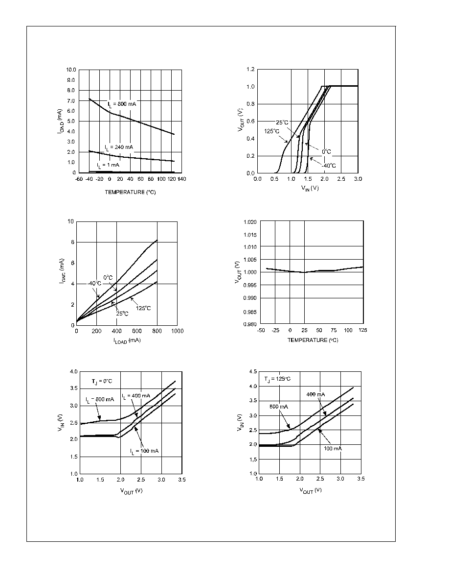
Typical Performance Characteristics
Unless otherwise specified: V
IN
= 3.3V, V
OUT
= 1V, I
L
= 1 mA,
C
IN
= 4.7 µF, C
OUT
= 10 µF, V
S/D
= 2V, C
BYP
= 10 nF, T
J
= 25∞C.
I
GND
vs Temperature
Minimum V
IN
Over Temperature
20120920
20120921
I
GND
vs I
Load
V
OUT
vs Temperature
20120922
20120959
Minimum V
IN
vs V
OUT
Minimum V
IN
vs V
OUT
20120951
20120952
LP3878-ADJ
www.national.com
5