LP38841
0.8A Ultra Low Dropout Linear Regulators
Stable with Ceramic Output Capacitors
General Description
The LP38841 is a high current, fast response regulator
which can maintain output voltage regulation with minimum
input to output voltage drop. Fabricated on a CMOS process,
the device operates from two input voltages: Vbias provides
voltage to drive the gate of the N-MOS power transistor,
while Vin is the input voltage which supplies power to the
load. The use of an external bias rail allows the part to
operate from ultra low Vin voltages. Unlike bipolar regula-
tors, the CMOS architecture consumes extremely low quies-
cent current at any output load current. The use of an
N-MOS power transistor results in wide bandwidth, yet mini-
mum external capacitance is required to maintain loop sta-
bility.
The fast transient response of these devices makes them
suitable for use in powering DSP, Microcontroller Core volt-
ages and Switch Mode Power Supply post regulators. The
parts are available in TO-220 and TO-263 packages.
Dropout Voltage: 75 mV (typ)
@
0.8A load current.
Quiescent Current: 30 mA (typ) at full load.
Shutdown Current: 30 nA (typ) when S/D pin is low.
Precision Output Voltage: 1.5% room temperature accu-
racy.
Features
n
Ideal for conversion from 1.8V or 1.5V inputs
n
Designed for use with low ESR ceramic capacitors
n
0.8V, 1.2V and 1.5V standard voltages available
n
Ultra low dropout voltage (75mV
@
0.8A typ)
n
1.5% initial output accuracy
n
Load regulation of 0.1%/A (typical)
n
30nA quiescent current in shutdown (typical)
n
Low ground pin current at all loads
n
Over temperature/over current protection
n
Available in 5 lead TO220 and TO263 packages
n
-40∞C to +125∞C junction temperature range
Applications
n
ASIC Power Supplies In:
- Desktops, Notebooks, and Graphics Cards, Servers
- Gaming Set Top Boxes, Printers and Copiers
n
Server Core and I/O Supplies
n
DSP and FPGA Power Supplies
n
SMPS Post-Regulator
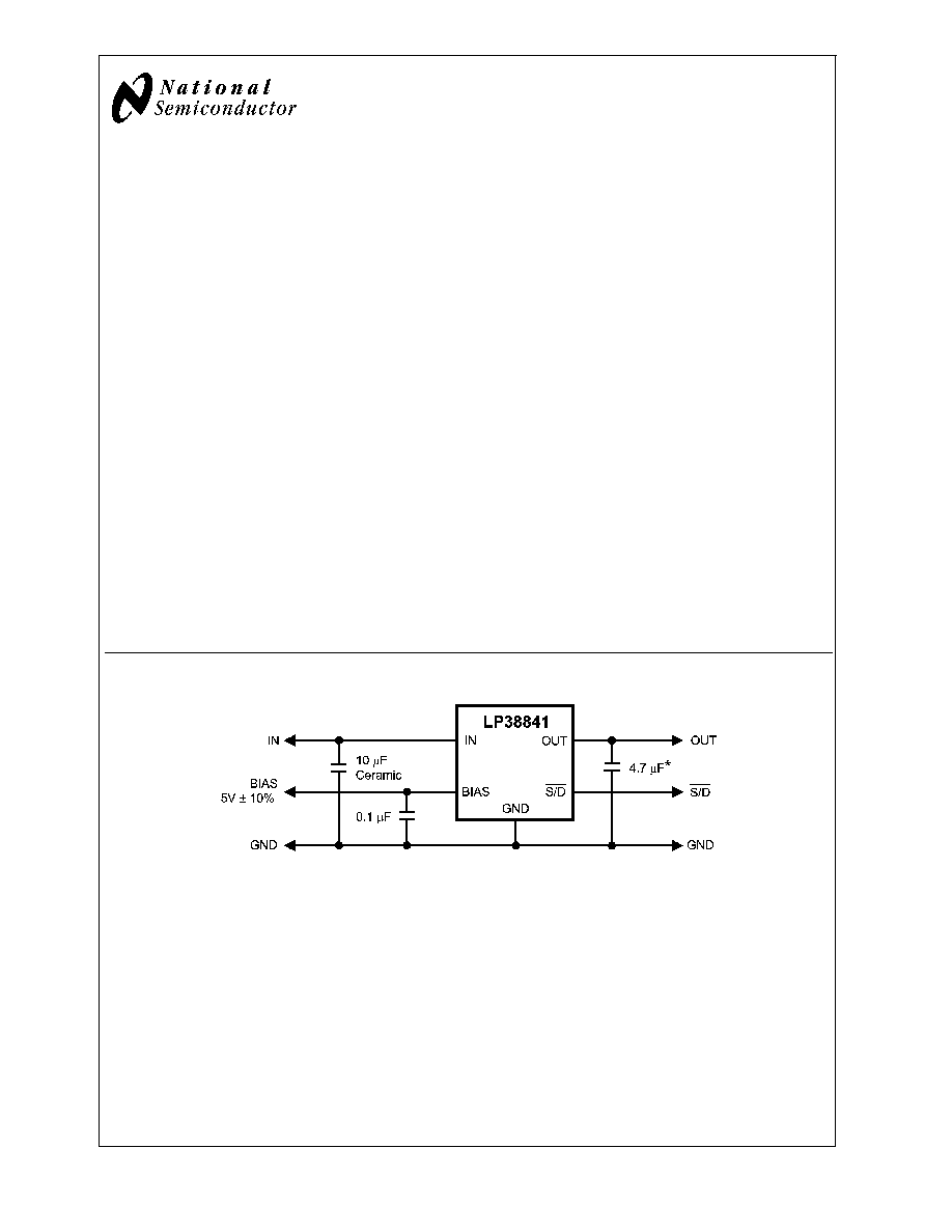
Typical Application Circuit
20102801
* Minimum value required if Tantalum capacitor is used (see Application Hints).
December 2004
LP38841
0.8A
Ultra
Low
Dropout
Linear
Regulators
Stable
with
Ceramic
Output
Capacitors
© 2004 National Semiconductor Corporation
DS201028
www.national.com
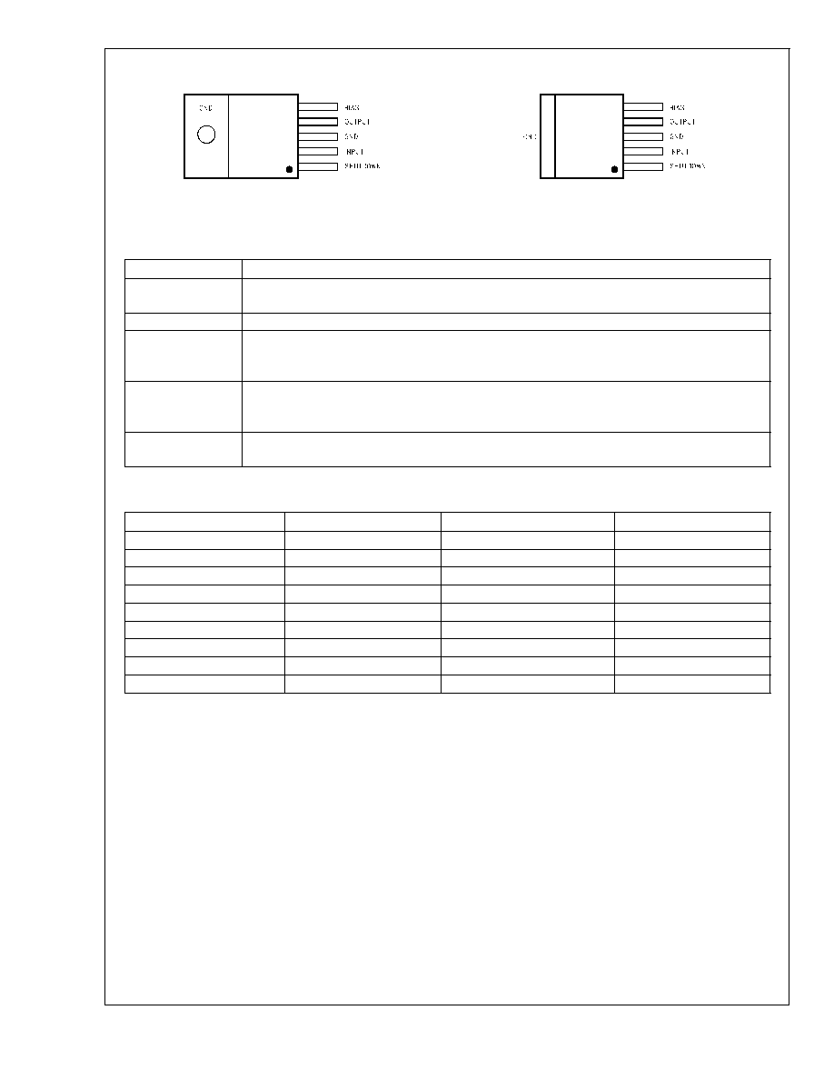
Connection Diagrams
20102802
TO-220, Top View
20102803
TO-263, Top View
Pin Description
Pin Name
Description
BIAS
The bias pin is used to provide the low current bias voltage to the chip which operates the internal
circuitry and provides drive voltage for the N-FET.
OUTPUT
The regulated output voltage is connected to this pin.
GND
This is both the power and analog ground for the IC. Note that both pin three and the tab of the
TO-220 and TO-263 packages are at ground potential. Pin three and the tab should be tied together
using the PC board copper trace material and connected to circuit ground.
INPUT
The high current input voltage which is regulated down to the nominal output voltage must be
connected to this pin. Because the bias voltage to operate the chip is provided seperately, the input
voltage can be as low as a few hundered millivolts above the output voltage.
SHUTDOWN
This provides a low power shutdown function which turns the regulated output OFF. Tie to V
BIAS
if
this function is not used.
Ordering Information
Order Number
Package Type
Package Drawing
Supplied As
LP38841S-0.8
TO263-5
TS5B
Rail
LP38841SX-0.8
TO263-5
TS5B
Tape and Reel
LP38841T-0.8
TO220-5
T05D
Rail
LP38841S-1.2
TO263-5
TS5B
Rail
LP38841SX-1.2
TO263-5
TS5B
Tape and Reel
LP38841T-1.2
TO220-5
T05D
Rail
LP38841S-1.5
TO263-5
TS5B
Rail
LP38841SX-1.5
TO263-5
TS5B
Tape and Reel
LP38841T-1.5
TO220-5
T05D
Rail
LP38841
www.national.com
2
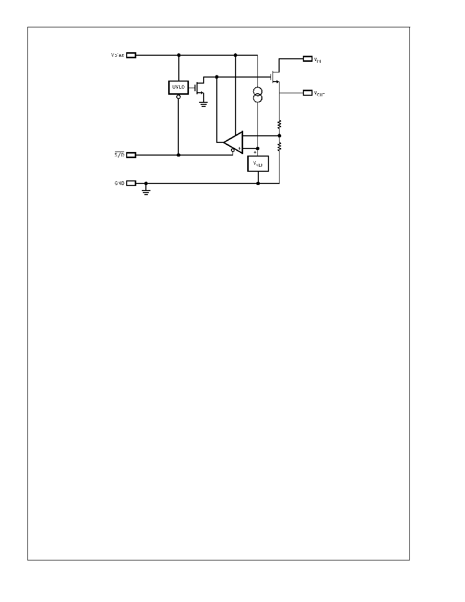
Block Diagram
20102824
LP38841
www.national.com
3
Absolute Maximum Ratings
(Note 1)
If Military/Aerospace specified devices are required,
please contact the National Semiconductor Sales Office/
Distributors for availability and specifications.
Storage Temperature Range
-65∞C to +150∞C
Lead Temp. (Soldering, 5 seconds)
260∞C
ESD Rating
Human Body Model (Note 3)
Machine Model (Note 9)
2 kV
200V
Power Dissipation (Note 2)
Internally Limited
V
IN
Supply Voltage (Survival)
-0.3V to +6V
V
BIAS
Supply Voltage (Survival)
-0.3V to +7V
Shutdown Input Voltage (Survival)
-0.3V to +7V
I
OUT
(Survival)
Internally Limited
Output Voltage (Survival)
-0.3V to +6V
Junction Temperature
-40∞C to +150∞C
Operating Ratings
V
IN
Supply Voltage
(V
OUT
+ V
DO
) to 5.5V
Shutdown Input Voltage
0 to +5.5V
I
OUT
0.8A
Operating Junction
Temperature Range
-40∞C to +125∞C
V
BIAS
Supply Voltage
4.5V to 5.5V
V
OUT
0.8V to 1.5V
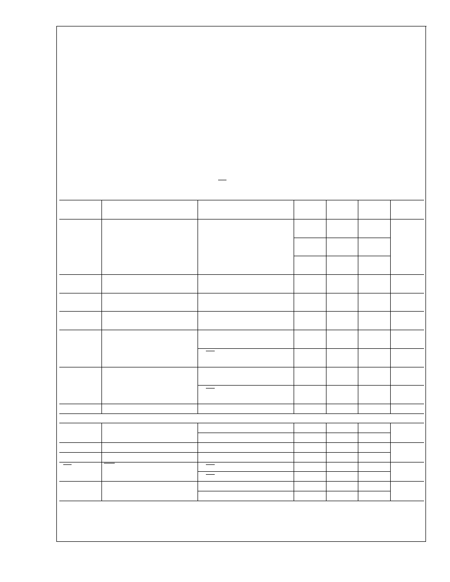
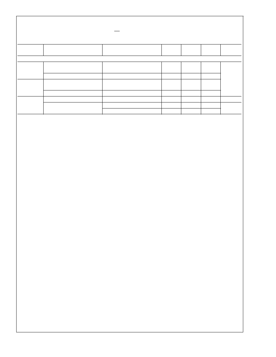
Electrical Characteristics
Limits in standard typeface are for T
J
= 25∞C, and limits in boldface type apply
over the full operating temperature range. Unless otherwise specified: V
IN
= V
O
(NOM) + 1V, V
BIAS
= 4.5V, I
L
= 10 mA, C
IN
=
10 µF CER, C
OUT
= 22 µF CER, C
BIAS
= 1 µF CER, V
S/D
= V
BIAS
. Min/Max limits are guaranteed through testing, statistical
correlation, or design.
Symbol
Parameter
Conditions
MIN
TYP
(Note 4)
MAX
Units
V
O
Output Voltage Tolerance
10 mA
<
I
L
<
0.8A
V
O
(NOM) + 1V
V
IN
5.5V
4.5V
V
BIAS
5.5V
0.788
0.776
0.8
0.812
0.824
V
1.182
1.164
1.2
1.218
1.236
1.478
1.455
1.5
1.523
1.545
V
O
/
V
IN
Output Voltage Line Regulation
(Note 6)
V
O
(NOM) + 1V
V
IN
5.5V
0.01
%/V
V
O
/
I
L
Output Voltage Load Regulation
(Note 7)
10 mA
<
I
L
<
0.8A
0.1
0.4
1.3
%/A
V
DO
Dropout Voltage (Note 8)
I
L
= 0.8A
75
120
205
mV
I
Q
(V
IN
)
Quiescent Current Drawn from
V
IN
Supply
10 mA
<
I
L
<
0.8A
30
35
40
mA
V
S/D
0.3V
0.06
1
30
µA
I
Q
(V
BIAS
)
Quiescent Current Drawn from
V
BIAS
Supply
10 mA
<
I
L
<
0.8A
2
4
6
mA
V
S/D
0.3V
0.03
1
30
µA
I
SC
Short-Circuit Current
V
OUT
= 0V
2.6
A
Shutdown Input
V
SDT
Output Turn-off Threshold
Output = ON
0.7
1.3
V
Output = OFF
0.3
0.7
Td (OFF)
Turn-OFF Delay
R
LOAD
X C
OUT
<<
Td (OFF)
20
µs
Td (ON)
Turn-ON Delay
R
LOAD
X C
OUT
<<
Td (ON)
15
I
S/D
S/D Input Current
V
S/D
=1.3V
1
µA
V
S/D
0.3V
-1
J-A
Junction to Ambient Thermal
Resistance
TO-220, No Heatsink
65
∞C/W
TO-263, 1 sq.in Copper
35
LP38841
www.national.com
4
Electrical Characteristics
Limits in standard typeface are for T
J
= 25∞C, and limits in boldface type apply
over the full operating temperature range. Unless otherwise specified: V
IN
= V
O
(NOM) + 1V, V
BIAS
= 4.5V, I
L
= 10 mA, C
IN
=
10 µF CER, C
OUT
= 22 µF CER, C
BIAS
= 1 µF CER, V
S/D
= V
BIAS
. Min/Max limits are guaranteed through testing, statistical
correlation, or design. (Continued)
Symbol
Parameter
Conditions
MIN
TYP
(Note 4)
MAX
Units
AC Parameters
PSRR (V
IN
)
Ripple Rejection for V
IN
Input
Voltage
V
IN
= V
OUT
+1V, f = 120 Hz
80
dB
V
IN
= V
OUT
+ 1V, f = 1 kHz
65
PSRR
(V
BIAS
)
Ripple Rejection for V
BIAS
Voltage
V
BIAS
= V
OUT
+ 3V, f = 120 Hz
58
V
BIAS
= V
OUT
+ 3V, f = 1 kHz
58
e
n
Output Noise Density
f = 120 Hz
1
µV/root-Hz
Output Noise Voltage
V
OUT
= 1.5V
BW = 10 Hz - 100 kHz
150
µV (rms)
BW = 300 Hz - 300 kHz
90
Note 1: Absolute maximum ratings indicate limits beyond which damage to the component may occur. Operating ratings indicate conditions for which the device
is intended to be functional, but do not guarantee specific performance limits. For guaranteed specifications, see Electrical Characteristics. Specifications do not
apply when operating the device outside of its rated operating conditions.
Note 2: At elevated temperatures, device power dissipation must be derated based on package thermal resistance and heatsink thermal values.
J-A
for TO-220
devices is 65∞C/W if no heatsink is used. If the TO-220 device is attached to a heatsink, a
J-S
value of 4∞C/W can be assumed.
J-A
for TO-263 devices is
approximately 35∞C/W if soldered down to a copper plane which is at least 1 square inch in area. If power dissipation causes the junction temperature to exceed
specified limits, the device will go into thermal shutdown.
Note 3: The human body model is a 100 pF capacitor discharged through a 1.5k resistor into each pin.
Note 4: Typical numbers represent the most likely parametric norm for 25∞C operation.
Note 5: If used in a dual-supply system where the regulator load is returned to a negative supply, the output pin must be diode clamped to ground.
Note 6: Output voltage line regulation is defined as the change in output voltage from nominal value resulting from a change in input voltage.
Note 7: Output voltage load regulation is defined as the change in output voltage from nominal value as the load current increases from no load to full load.
Note 8: Dropout voltage is defined as the minimum input to output differential required to maintain the output with 2% of nominal value.
Note 9: The machine model is a 220 pF capacitor discharged directly into each pin.
LP38841
www.national.com
5