LP38859
3A Fast-Response High-Accuracy LDO Linear Regulator
with Soft-Start
General Description
The LP38859 is a high current, fast response regulator
which can maintain output voltage regulation with extremely
low input to output voltage drop. Fabricated on a CMOS
process, the device operates from two input voltages: V
BIAS
provides voltage to drive the gate of the N-MOS power
transistor, while V
IN
is the input voltage which supplies
power to the load. The use of an external bias rail allows the
part to operate from ultra low V
IN
voltages. Unlike bipolar
regulators, the CMOS architecture consumes extremely low
quiescent current at any output load current. The use of an
N-MOS power transistor results in wide bandwidth, yet mini-
mum external capacitance is required to maintain loop sta-
bility.
The fast transient response of this device makes it suitable
for use in powering DSP, Microcontroller Core voltages and
Switch Mode Power Supply post regulators. The LP38859 is
available in TO-220 and TO-263 5-Lead packages.
Dropout Voltage: 240 mV (typical) at 3A load current.
Low Ground Pin Current: 14 mA (typical) at 3A load cur-
rent.
Soft-Start: Programmable Soft-Start time.
Precision Output Voltage:
±
1.0% for T
J
= 25∞C and
±
2.0%
for 0∞C
T
J
+125∞C, across all line and load conditions
Features
n
Standard V
OUT
values of 0.8V and 1.2V
n
Stable with 10µF Ceramic capacitors
n
Dropout voltage of 240 mV (typical) at 3A load current
n
Precision Output Voltage across all line and load
conditions:
--
±
1.0% V
OUT
for T
J
= 25∞C
--
±
2.0% V
OUT
for 0∞C
T
J
+125∞C
--
±
3.0% V
OUT
for -40∞C
T
J
+125∞C
n
Over-Temperature and Over-Current protection
n
Available in 5 lead TO-220 and TO-263 packages
n
Custom V
OUT
values between 0.8V and 1.2V are
available
n
-40∞C to +125∞C Operating Temperature Range
Applications
n
ASIC Power Supplies In:
- Desktops, Notebooks, and Graphics Cards, Servers
- Gaming Set Top Boxes, Printers and Copiers
n
Server Core and I/O Supplies
n
DSP and FPGA Power Supplies
n
SMPS Post-Regulator
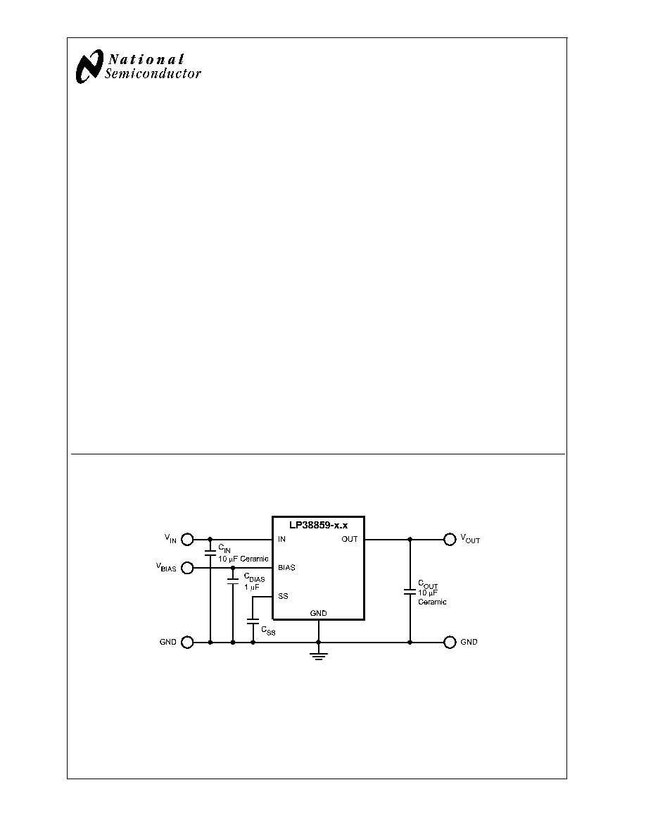
Typical Application Circuit
20131201
June 2006
LP38859
3A
Fast-Response
High-Accuracy
LDO
Linear
Regulator
with
Soft-Start
© 2006 National Semiconductor Corporation
DS201312
www.national.com
Ordering Information
V
OUT
*
Order Number
Package Type
Package Drawing
Supplied As
0.8V
LP38859S-0.8
TO263-5
TS5B
Rail of 45
LP38859SX-0.8
TO263-5
TS5B
Tape and Reel of 500
LP38859T-0.8
TO220-5
T05D
Rail of 45
1.2V
LP38859S-1.2
TO263-5
TS5B
Rail of 45
LP38859SX-1.2
TO263-5
TS5B
Tape and Reel of 500
LP38859T-1.2
TO220-5
T05D
Rail of 45
* For custom V
OUT
values between 0.8V and 1.2V please contact the National Semiconductor Sales Office.
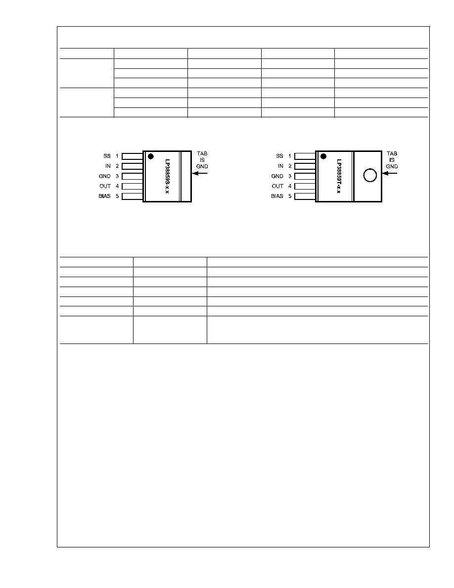
Connection Diagrams
20131202
TO263≠5, Top View
20131203
TO220≠5, Top View
Pin Descriptions
TO220≠5 and TO263≠5 Packages
Pin #
Pin Symbol
Pin Description
1
SS
Soft-Start capacitor connection. Used to slow the rise time of V
OUT
at turn-on.
2
IN
The unregulated voltage input pin.
3
GND
Ground
4
OUT
The regulated output voltage pin.
5
BIAS
The supply for the internal control and reference circuitry.
TAB
TAB
The TAB is a thermal connection that is physically attached to the backside of
the die, and used as a thermal heat-sink connection. See the Application
Information section for details.
LP38859
www.national.com
2
Absolute Maximum Ratings
(Note 1)
If Military/Aerospace specified devices are required,
please contact the National Semiconductor Sales Office/
Distributors for availability and specifications.
Storage Temperature Range
-65∞C to +150∞C
Lead Temperature
Soldering, 5 seconds
260∞C
ESD Rating
Human Body Model (Note 2)
±
2 kV
Power Dissipation (Note 3)
Internally Limited
V
IN
Supply Voltage (Survival)
-0.3V to +6.0V
V
BIAS
Supply Voltage (Survival)
-0.3V to +6.0V
V
SS
SoftStart Voltage (Survival)
-0.3V to +6.0V
V
OUT
Voltage (Survival)
-0.3V to +6.0V
I
OUT
Current (Survival)
Internally Limited
Junction Temperature
-40∞C to +150∞C
Operating Ratings
(Note 1)
V
IN
Supply Voltage
(V
OUT
+ V
DO
) to V
BIAS
V
BIAS
Supply Voltage
3.0V to 5.5V
I
OUT
0 mA to 3.0A
Junction Temperature
Range(Note 3)
-40∞C to +125∞C
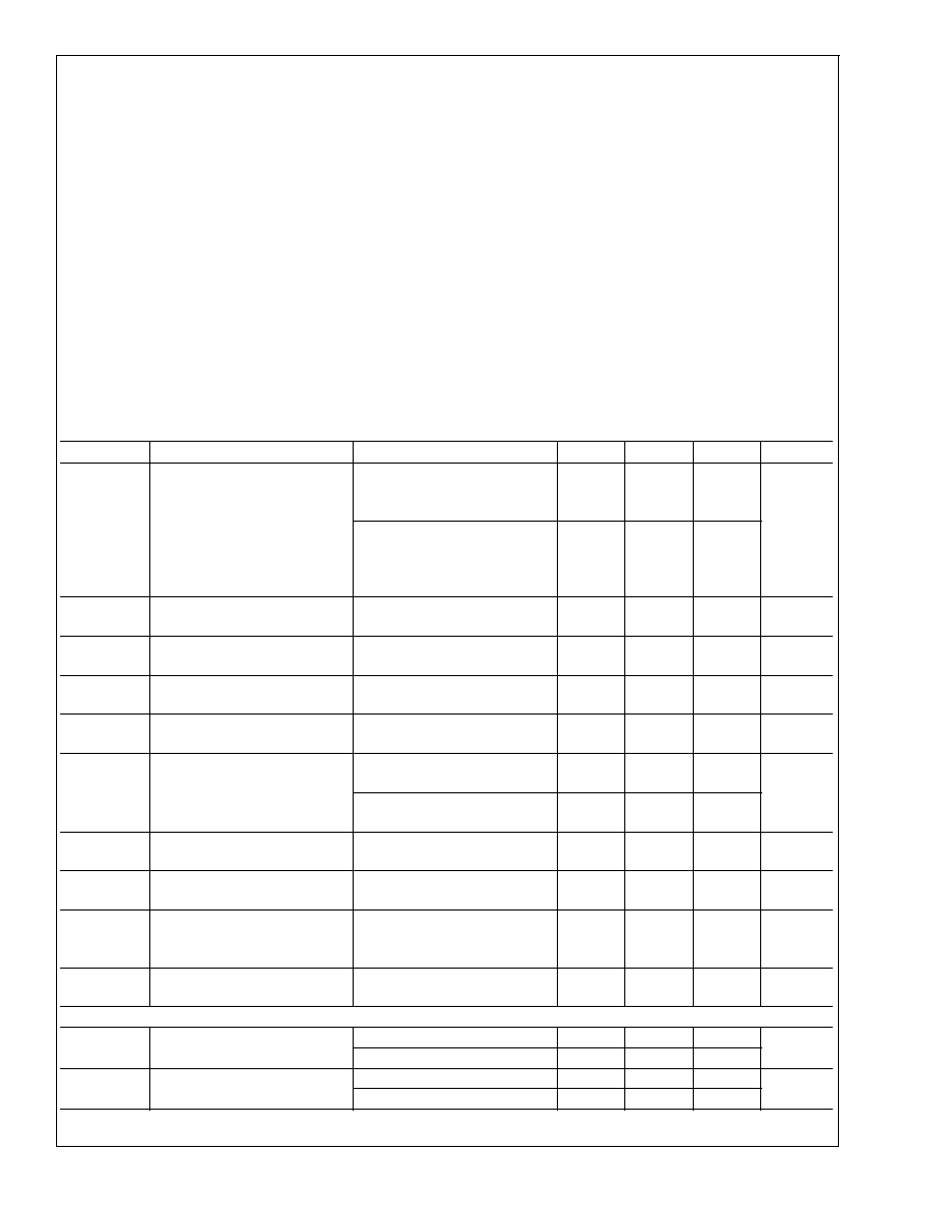
Electrical Characteristics
Unless otherwise specified: V
IN
= V
OUT(NOM)
+ 1V, V
BIAS
= 3.0V, I
OUT
= 10 mA,
C
IN
= C
OUT
= 10 µF, C
BIAS
= 1 µF, C
SS
= open. Limits in standard type are for T
J
= 25∞C only; limits in boldface type apply
over the junction temperature (T
J
) range of -40∞C to +125∞C. Minimum and Maximum limits are guaranteed through test, de-
sign, or statistical correlation. Typical values represent the most likely parametric norm at T
J
= 25∞C, and are provided for ref-
erence purposes only.
Symbol
Parameter
Conditions
MIN
TYP
MAX
Units
V
OUT
V
OUT
Accuracy
V
OUT(NOM)
+ 1V
V
IN
V
BIAS
,
3.0V
V
BIAS
5.5V,
10 mA
I
OUT
3A
-1.0
-3.0
0.0
1.0
3.0
%
V
OUT(NOM)
+ 1V
V
IN
V
BIAS
,
3.0V
V
BIAS
5.5V,
10 mA
I
OUT
3.0A,
0∞C
T
J
+125∞C
-2.0
0.0
2.0
V
OUT
/
V
IN
Line Regulation, V
IN
(Note 4)
V
OUT(NOM)
+ 1V
V
IN
V
BIAS
-
0.04
-
%/V
V
OUT
/
V
BIAS
Line Regulation, V
BIAS
(Note 4)
3.0V
V
BIAS
5.5V
-
0.10
-
%/V
V
OUT
/
I
OUT
Output Voltage Load Regulation
(Note 5)
10 mA
I
OUT
3.0A
-
0.2
-
%/A
V
DO
Dropout Voltage (Note 6)
I
OUT
= 3.0A
-
240
300
450
mV
I
GND(IN)
Quiescent Current Drawn from
V
IN
Supply
LP38859-0.8
10 mA
I
OUT
3.0A
-
7.0
8.5
9.0
mA
LP38859-1.2
10 mA
I
OUT
3.0A
11
12
15
I
GND(BIAS)
Quiescent Current Drawn from
V
BIAS
Supply
10 mA
I
OUT
3.0A
-
3.0
3.8
4.5
mA
UVLO
Under-Voltage Lock-Out
Threshold
V
BIAS
rising until device is
functional
2.20
2.00
2.45
2.70
2.90
V
UVLO
(HYS)
Under-Voltage Lock-Out
Hysteresis
V
BIAS
falling from UVLO
threshold until device is
non-functional
60
50
150
300
350
mV
I
SC
Output Short-Circuit Current
V
IN
= V
OUT(NOM)
+ 1V,
V
BIAS
= 3.0V, V
OUT
= 0.0V
-
6.2
-
A
Soft-Start
r
SS
Soft-Start internal resistance
LP38859-0.8
11.0
13.5
16.0
k
LP38859-1.2
13.5
16.0
18.5
t
SS
Soft-Start time
t
SS
= C
SS
x r
SS
x 5
LP38859-0.8, C
SS
= 10 nF
-
675
-
µs
LP38859-1.2, C
SS
= 10 nF
-
800
-
LP38859
www.national.com
3
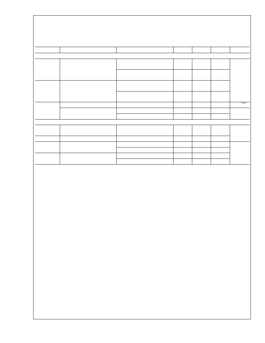
Electrical Characteristics
Unless otherwise specified: V
IN
= V
OUT(NOM)
+ 1V, V
BIAS
= 3.0V, I
OUT
= 10 mA,
C
IN
= C
OUT
= 10 µF, C
BIAS
= 1 µF, C
SS
= open. Limits in standard type are for T
J
= 25∞C only; limits in boldface type apply
over the junction temperature (T
J
) range of -40∞C to +125∞C. Minimum and Maximum limits are guaranteed through test,
design, or statistical correlation. Typical values represent the most likely parametric norm at T
J
= 25∞C, and are provided for
reference purposes only. (Continued)
Symbol
Parameter
Conditions
MIN
TYP
MAX
Units
AC Parameters
PSRR
(V
IN
)
Ripple Rejection for V
IN
Input
Voltage
V
IN
= V
OUT(NOM)
+ 1V,
f = 120 Hz
-
80
-
dB
V
IN
= V
OUT(NOM)
+ 1V,
f = 1 kHz
-
65
-
PSRR
(V
BIAS
)
Ripple Rejection for V
BIAS
Voltage
V
BIAS
= V
OUT(NOM)
+ 3V,
f = 120 Hz
-
58
-
V
BIAS
= V
OUT(NOM)
+ 3V,
f = 1 kHz
-
58
-
e
n
Output Noise Density
f = 120 Hz
-
1
-
µV/
Hz
Output Noise Voltage
V
OUT
= 1.8V
BW = 10 Hz - 100 kHz
-
150
-
µV (rms)
BW = 300 Hz - 300 kHz
-
90
-
Thermal Parameters
T
SD
Thermal Shutdown Junction
Temperature
-
160
-
∞C
T
SD(HYS)
Thermal Shutdown Hysteresis
-
10
-
J-A
Thermal Resistance, Junction to
Ambient(Note 3)
TO220-5
-
60
-
∞C/W
TO263-5
-
60
-
J-C
Thermal Resistance, Junction to
Case(Note 3)
TO220-5
-
3
-
TO263-5
-
3
-
Note 1: Note 1: Absolute Maximum Ratings indicate limits beyond which damage to the device may occur. Operating Ratings indicate conditions for which the
device is intended to be functional, but does not guarantee specific performance limits. For guaranteed specifications and conditions, see the Electrical
Characteristics.
Note 2: The human body model is a 100 pF capacitor discharged through a 1.5k resistor into each pin. Test method is per JESD22-A114. The HBM rating for device
pin 1 (SS) is
±
1.5 kV.
Note 3: Device power dissipation must be de-rated based on device power dissipation (P
D
), ambient temperature (T
A
), and package junction to ambient thermal
resistance (
JA
). Additional heat-sinking may be required to ensure that the device junction temperature (T
J
) does not exceed the maximum operating rating. See
the Application Information section for details.
Note 4: Output voltage line regulation is defined as the change in output voltage from nominal value resulting from a change in input voltage.
Note 5: Output voltage load regulation is defined as the change in output voltage from nominal value as the load current increases from no load to full load.
Note 6: Dropout voltage is defined the as input to output voltage differential (V
IN
- V
OUT
) where the input voltage is low enough to cause the output voltage to drop
no more than 2% from the nominal value.
LP38859
www.national.com
4
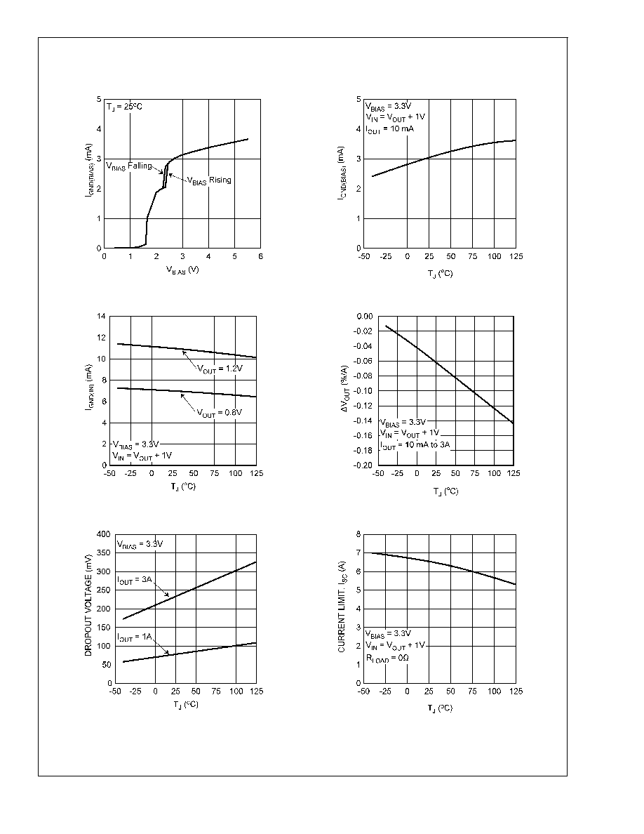
Typical Performance Characteristics
Unless otherwise specified: T
J
= 25∞C, V
IN
= V
OUT(NOM)
+ 1V,
V
BIAS
= 3.0V, I
OUT
= 10 mA, C
IN
= C
OUT
= 10 µF Ceramic, C
BIAS
= 1 µF Ceramic, C
SS
= open.
V
BIAS
Ground Pin Current (I
GND(BIAS)
) vs V
BIAS
V
BIAS
Ground Pin Current (I
GND(BIAS)
) vs Temperature
20131287
20131261
V
IN
Ground Pin Current vs Temperature
Load Regulation vs Temperature
20131262
20131263
Dropout Voltage (V
DO
) vs Temperature
Output Current Limit (I
SC
) vs Temperature
20131265
20131266
LP38859
www.national.com
5