LP3927
Cellular/PCS System Power Management IC
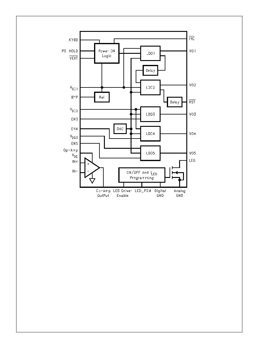
General Description
The LP3927 system power management IC is designed for
cellular/PCS handsets as well as other portable systems that
require intelligent power management. Each device contains
five low-dropout linear regulators (LDO's), a reset timer, a
power-up control logic, a general-purpose open drain output
that can be used to light LEDs, and a CMOS rail-to-rail
input/output operational amplifier.
Each linear regulator features an extremely low dropout
voltage of 100 mV (typ) at maximum output current. LDO1
and LDO2 are powered on and off by either the KYBD or the
VEXT pin. LDO3, LDO4 and LDO5 each have its indepen-
dent enable pin. LDO1 and LDO4 are rated at 150 mA each,
LDO2 and LDO5 are rated at 200 mA each and LDO3 is
rated at 100 mA. All LDO's are optimized for low noise and
high isolation.
The open drain output current sink can be programmed up to
150 mA by using an external low cost resistor.
A single supply, low voltage operational amplifier has rail to
rail input and output with 600 kHz of gain-bandwidth product.
Key Specifications
n
3.0V to 5.5V Input Voltage Range
n
Two 200 mA, Two 150 mA and One 100 mA LDO's
n
100 mV typ Dropout Voltage
@
I
MAX
n
150 mA General-Purpose Open-drain programmable
current sink for back light LED
n
Low Voltage Rail to Rail Input/Output Operational
Amplifier
n
28 pin LLP package
Applications
n
Cellular/PCS handsets
n
PDA's, Palmtops, and portable terminals
n
Single�Cell Li+ Systems
n
2- or 3- Cell NiMH, NiCd or Alkaline System
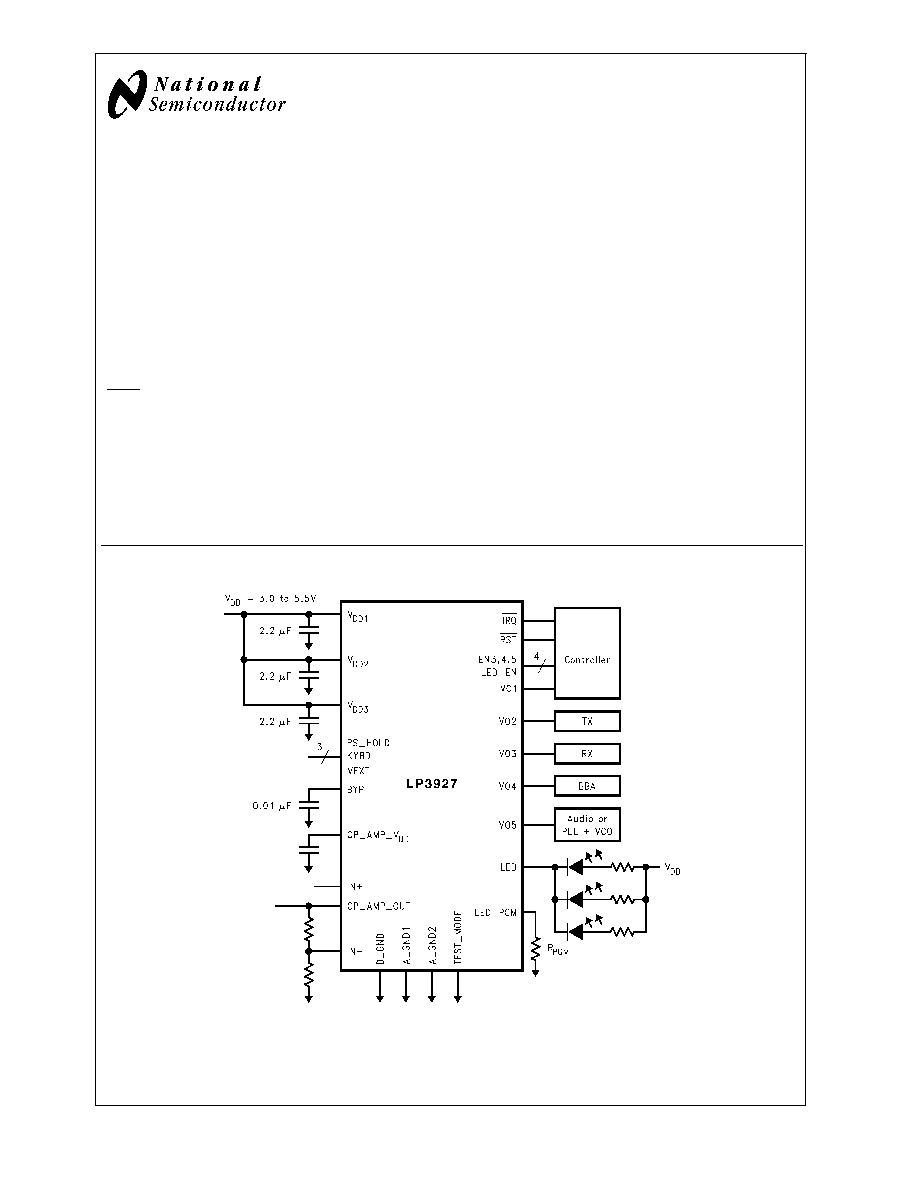
Typical Application Circuit
20037901
V
DD1
, V
DD2
and V
DD3
must be tied together externally. Collectively called V
DD
.
December 2005
LP3927
Cellular/PCS
System
Power
Management
IC
� 2005 National Semiconductor Corporation
DS200379
www.national.com
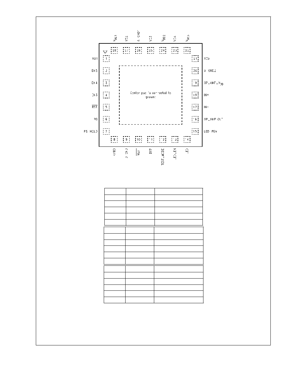
LP3927 Pin Out Diagram (Top View)
20037902
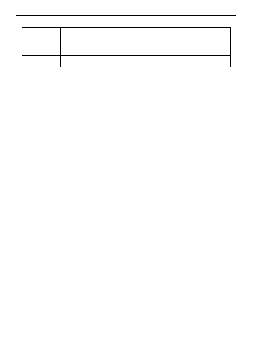
Output Current Rating and Voltage Options
I
MAX
(mA)
Voltage Options (V)
LDO1
150
1.8, 1.9, 2.5, 2.6*, 2.7
LDO2
200
1.8, 2.85*, 2.9, 3.0
LDO3
100
2.7, 2.8, 2.9*, 3.0
LDO4
150
2.7, 2.8, 2.9*, 3.0
LDO5
200
2.7, 2.8, 2.9, 3.0*
I
MAX
(mA)
Voltage Options (V)
LDO1
150
1.85*, 1.9, 2.5, 2.6, 2.7
LDO2
200
1.8, 2.85*, 2.9, 3.0
LDO3
100
2.7, 2.85*, 2.9, 3.0
LDO4
150
2.6*, 2.85, 2.9, 3.0
LDO5
200
2.7, 2.85*, 2.9, 3.0
I
MAX
(mA)
Voltage Options (V)
LDO1
150
1.85*, 1.9, 2.5, 2.6, 2.7
LDO2
200
1.8, 2.85, 2.9, 3.0*
LDO3
100
2.7, 2.85, 2.9, 3.0*
LDO4
150
2.6, 2.85, 2.9, 3.0*
LDO5
200
2.7, 2.85, 2.9, 3.0*
* denotes the voltage options that are available currently. For other options, please contact the
National Semiconductor factory sales office/distributors for availability and specifications.
Voltage options in the two tables cannot be mixed and matched.
LP3927
www.national.com
2

Pin Descriptions
Pin
Name
Functional Description
1
VO1
150 mA, LDO1 output pin.
2
EN5
LDO5 enable input.
3
EN4
LDO4 enable input.
4
EN3
LDO3 enable input.
5
RST
Externally pulled high, open drain output to processor/memory reset.
6
IRQ
Externally pulled high, open drain output to processor interrupt indicating KYBD has gone
high.
7
PS_HOLD
Input from the processor to the LP3927. A HIGH indicates a steady supply of power is
granted. Refer to "Application Hints" section for more detail.
8
KYBD
An active high input signal indicating the keyboard "On/Off" button has been asserted. Refer
to "Application Hints" section for more detail.
9
D_GND
Digital ground, used primarily for the digital and DAC circuits.
10
VEXT
Active low input indicating a battery charger insertion Refer to "Application Hints" section for
more detail.
11
BYP
Reference bypass pin.
12
TEST_MODE
Pin used for production testing, factory use only. This pin should be grounded in applications.
13
LED_EN
LED driver enable input.
14
LED
LED driver, drain connection of the LED drive MOSFET.
15
LED_PGM
LED drive current programming pin.
16
OP_AMP_OUT
Operational amplifier output pin.
17
IN-
- input of the Op-Amp.
18
IN+
+ input of the Op-Amp.
19
OP_AMP_V
DD
Power supply pin for Op-Amp.
20
A_GND2
Ground for analog.
21
VO5
200 mA, LDO5 output pin.
22
V
DD3
Input power pin for LDO5. V
DD1
, V
DD2
and V
DD3
must be tied together externally.
23
VO4
150 mA, LDO4 output pin.
24
V
DD2
Input power pin for LDO3 and LDO4. V
DD1
, V
DD2
and V
DD3
must be tied together externally.
25
VO3
100 mA, LDO3 output pin.
26
A_GND1
Ground for analog.
27
VO2
200 mA, LDO2 output pin.
28
V
DD1
Input power pin for LDO1 and LDO2. V
DD1
, V
DD2
and V
DD3
must be tied together externally.
LP3927
www.national.com
4