 | –≠–ª–µ–∫—Ç—Ä–æ–Ω–Ω—ã–π –∫–æ–º–ø–æ–Ω–µ–Ω—Ç: LP3936SLX | –°–∫–∞—á–∞—Ç—å:  PDF PDF  ZIP ZIP |
LP3936
Lighting Management System for Six White LEDs and
One RGB or FLASH LED
General Description
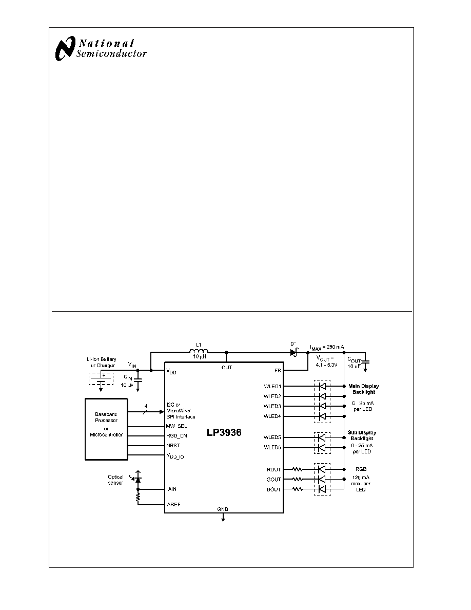
LP3936 is a complete lighting management system de-
signed for portable wireless applications. It contains a boost
DC/DC converter, 4 white LED drivers to drive the main LCD
panel backlight, 2 white LED drivers for sub-LCD panel and
1 set of RGB LED drivers.
Both WLED groups have 8-bit programmable constant cur-
rent drivers that are separately adjustable and matched to
1% (typ.). For efficient backlighting the backlight intensity
can be adjusted using the 8-bit ADC with ambient light
detection circuit.
The RGB LED drivers are PWM-driven with programmable
color, intensity and blinking patterns. In addition, they feature
a FLASH function to support picture taking with camera-
enabled cellular phones.
An efficient magnetic boost converter provides the required
bias operating from a single Li-Ion battery. The DC/DC con-
verter output voltage is user programmable for adapting to
different LED types and for efficiency optimization. All func-
tions
are
software
controllable
through
an
I
2
C
and
MicroWire/SPI compatible interface and 16 internal regis-
ters.
Features
n
High Efficiency 250 mA Magnetic Boost DC-DC
Converter with Programmable Output Voltage
n
PWM controlled RGB LED drivers with programmable
color, brightness, turn on/off slopes and blinking
n
FLASH function with 3 drivers, each up to 120 mA
current
n
4 constant current White LED drivers with
programmable 8-bit adjustment (0 ... 25 mA/LED)
n
2 constant current White LED drivers with
programmable 8-bit adjustment (0 ... 25 mA/LED)
n
8-bit ADC for ambient light sensor with averaging
n
Combined MicroWire/SPI and I
2
C compatible serial
interface
n
Low current Standby mode (software controlled)
n
Low voltage digital interface down to 1.8V
n
Space efficient 32-pin thin CSP laminate package
Applications
n
Cellular Phones
n
PDAs
Typical Application
20081401
June 2004
LP3936
Lighting
Management
System
for
Six
White
LEDs
and
One
RGB
or
FLASH
LED
© 2004 National Semiconductor Corporation
DS200814
www.national.com
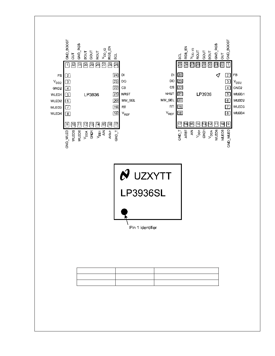
Connection Diagrams and Package Mark Information
32-Lead Thin CSP Package, 4.5 x 5.5 x 0.8 mm, 0.5 mm pitch
See NS Package Number SLD32A
20081402
Top View
20081403
Bottom View
20081404
Note: The actual physical placement of the package marking will vary from part to part. The package marking "XY" designates the date code. "UZ" and "TT" are NSC
internal codes for die manufacturing and assembly traceability. Both will vary considerably.
Package Mark -- Top View
Ordering Information
Order Number
Package Marking
Supplied As
LP3936SL
LP3936SL
1000 units, Tape-and-Reel
LP3936SLX
LP3936SL
2500 units, Tape-and-Reel
LP3936
www.national.com
2
Pin Description
Pin
Name
Type
Description
1
GND_BOOST
Ground
Power Switch Ground
2
FB
Input
Boost Converter Feedback
3
V
DD2
Power
Supply Voltage for Internal Digital Circuits
4
GND2
Ground
Ground Return for V
DD2
(Internal Digital)
5
WLED1
LED Output
Open Drain, White LED1 Output
6
WLED2
LED Output
Open Drain, White LED2 Output
7
WLED3
LED Output
Open Drain, White LED3 Output
8
WLED4
LED Output
Open Drain, White LED4 Output
9
GND_WLED
Ground
4+2 White LED Driver Ground
10
WLED5
LED Output
Open Drain, White LED5 Output
11
WLED6
LED Output
Open Drain, White LED6 Output
12
V
DDA
Output
Internal LDO Output, 2.8V
13
GND1
Ground
Ground Return for V
DD1
(Internal Analog)
14
V
DD1
Power
Supply Voltage for Internal Analog Circuits
15
AIN
Input
Ambient Light Sensor Input
16
AREF
Output
Reference Voltage for Ambient Light Sensor, 1.23V
17
GND_T
Ground
Ground
18
V
REF
Output
Internal Reference Bypass Capacitor
19
RT
Input
Oscillator Resistor
20
MW_SEL
Logic Input
MicroWire -- I
2
C select (MW_SEL=1 in MicroWire Mode)
21
NRST
Logic Input
Low Active Reset Input
22
CS
Logic
Input/Output
MicroWire Chip-Select (in) / I
2
C SDA (in/out)
23
DO
Logic Output
MicroWire Data Output
24
DI
Logic Input
MicroWire Data Input
25
SCL
Logic Input
MicroWire Clock / I
2
C SCL Input
26
RGB_EN
Logic Input
LED Control for On/Off or PWM Dimming
27
V
DD_IO
Power
Supply Voltage for Logic IO signals
28
ROUT
LED Output
Open Drain Output, Red LED
29
GOUT
LED Output
Open Drain Output, Green LED
30
BOUT
LED Output
Open Drain Output, Blue LED
31
GND_RGB
Ground
Ground for RGB Drivers
32
OUT
Output
Open Drain, Boost Converter Power Switch
LP3936
www.national.com
3

Absolute Maximum Ratings
(Notes 1,
2)
If Military/Aerospace specified devices are required,
please contact the National Semiconductor Sales Office/
Distributors for availability and specifications.
V
DD1
, V
DD2
, V
DD_IO
, V(OUT, FB)
-0.3V to 6.0V
Voltage on Logic Pins
-0.3V to V
DD_IO
+
0.3V, with 6.0V max
Voltage on LED Output Pins
-0.3V to V(FB) +
0.3V, with 6.0V max
Voltage on All Other Pins
-0.3V to V
DD1,2
+
0.3V, with 6.0V max
I (ROUT, GOUT, BOUT)
150 mA
I (V
REF
)
10 µA
Continuous Power Dissipation
(Note 3)
Internally Limited
Junction Temperature (T
J-MAX
)
125∞C
Storage Temperature Range
-65∞C to +150∞C
Maximum Lead Temperature
260∞C
(Reflow soldering, 3 times) (Note 4)
ESD Rating (Note 5)
Human Body Model:
2 kV
Machine Model:
200V
Operating Ratings
(Notes 1, 2)
V
DD1
, V
DD2
3.0V to 6.0V
V
DD_IO
1.8V ≠ V
DD1,2
Recommended Load Current
0 mA to 250 mA
Junction Temperature (T
J
) Range
-40∞C to +125∞C
Ambient Temperature (T
A
) Range
(Note 6)
-40∞C to +85∞C
Thermal Properties
Junction-to-Ambient Thermal Resistance (
JA
),
SLD32A Package (Note 7)
72∞C/W
Electrical Characteristics
(Notes 2, 8)
Limits in standard typeface are for T
J
= 25∞C. Limits in boldface type apply over the operating ambient temperature range
(-40∞C
T
A
+85∞C). Unless otherwise noted, specifications apply to the Section Block Diagram with: V
DD1
= V
DD2
= V
DD_IO
= 3.6V, C
VDD1
, C
VDD2
, C
VDDIO
= 1 µF, C
IN
, C
OUT
= 10 µF, C
VDDA
= 1 µF, C
VREF
= 0.1 µF, L
BOOST
= 10 µH (Note 9).
Symbol
Parameter
Condition
Min
Typ
Max
Units
V
DD1,2
Supply Voltage
3.0
3.6
6.0
V
I
DD
Standby Supply Current
(V
DD1
and V
DD2
current)
NSTBY = L (register)
CS, SCL, DI, NRST = H
V
DD1
, V
DD2
= 3.6V
1
7
µA
No-Load Supply Current
(V
DD1
and V
DD2
current, boost off)
NSTBY = H (reg.)
EN_BOOST = L (reg.)
SCL, CS, DI, NRST = H
170
300
µA
Full Load Supply Current
(V
DD1
and V
DD2
current, boost on)
NSTBY = H (register)
NRST, CS, SCL, DI = H
RGB_EN = L
WLED1 ... 6 = L
EN_AMBADC = L
1
mA
I
DD_IO
V
DD_IO
Standby Supply Current
NSTBY = L (register)
CS, SCL, DI, NRST = H
1
µA
V
DD_IO
Operating Supply Current
1 MHz Clock Frequency
C
L
= 50 pF at DO pin
20
µA
V
REF
Reference Voltage (Note 10)
I
REF
1 nA,
Test Purposes Only
1.205
-2
1.23
1.255
+2
V
%
V
DDA
LDO Output Voltage
IV
DDA
<
1 µA
2.688
≠4
2.8
2.912
+4
% V
Note 1: Absolute Maximum Ratings indicate limits beyond which damage to the component may occur. Operating Ratings are conditions under which operation of
the device is guaranteed. Operating Ratings do not imply guaranteed performance limits. For guaranteed performance limits and associated test conditions, see the
Electrical Characteristics tables.
Note 2: All voltages are with respect to the potential at the GND pins (GND1, GND2, GND_T, GND_BOOST, GND_WLED, GND_RGB).
Note 3: Internal thermal shutdown circuitry protects the device from permanent damage. Thermal shutdown engages at T
J
= 160∞C (typ.) and disengages at T
J
=
140∞C (typ.).
Note 4: For detailed soldering specifications and information, please refer to National Semiconductor Application Note 1125: Laminate CSP/FBGA
Package (AN-1125).
Note 5: The Human body model is a 100 pF capacitor discharged through a 1.5 k
resistor into each pin. The machine model is a 200 pF capacitor discharged
directly into each pin. MIL-STD-883 3015.7
LP3936
www.national.com
4
Electrical Characteristics
(Notes 2, 8) (Continued)
Note 6: In applications where high power dissipation and/or poor package thermal resistance is present, the maximum ambient temperature may have to be
derated. Maximum ambient temperature (T
A-MAX
) is dependent on the maximum operating junction temperature (T
J-MAX-OP
= 125∞C), the maximum power
dissipation of the device in the application (P
D-MAX
), and the junction-to ambient thermal resistance of the part/package in the application (
JA
), as given by the
following equation: T
A-MAX
= T
J-MAX-OP
- (
JA
x P
D-MAX
).
Note 7: Junction-to-ambient thermal resistance is highly application and board-layout dependent. In applications where high maximum power dissipation exists,
special care must be paid to thermal dissipation issues in board design.
Note 8: Min and Max limits are guaranteed by design, test, or statistical analysis. Typical numbers are not guaranteed, but do represent the most likely norm.
Note 9: Low-ESR Surface-Mount Ceramic Capacitors (MLCCs) are used in setting electrical characteristics.
Note 10: V
REF
pin (Bandgap reference output) is for internal use only. A capacitor should always be placed between V
REF
and GND1.
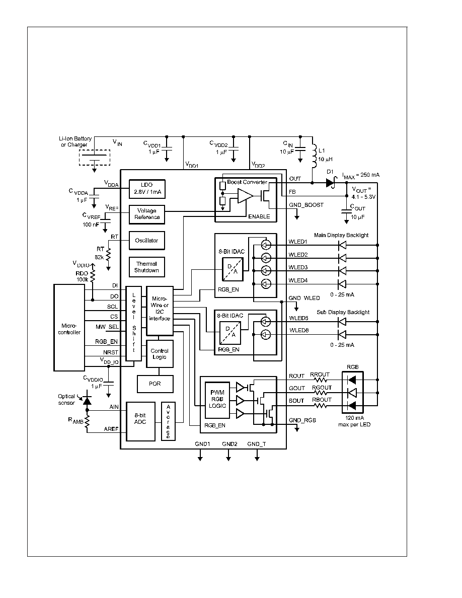
Block Diagram
20081405
LP3936
www.national.com
5