Äîêóìåíòàöèÿ è îïèñàíèÿ www.docs.chipfind.ru
LP3941A
Cellular Phone Power Management Unit
General Description
LP3941A is a complete power management IC designed for
a cellular phone. It contains 11 low noise low dropout regu-
lators, a linear charger for Li-Ion battery, a backup battery
charger, real time clock supply regulator, three open drain
drivers, two comparators and high speed I
2
C compatible
serial interface to program individual regulator output volt-
ages as well as on/off control.
LP3941 is available in a LLP48 package.
Features
n
11 low dropout, low noise LDOs.
n
Dedicated low current LDO for real time clock supply.
n
Back-up battery charger
n
A constant current / constant voltage battery charger
controller with charge status indication via I
2
C
compatible interface.
n
Three open drain drivers to control a RGB LED
n
I
2
C compatible serial interface for maximum flexibility
Applications
n
GSM/EDGE cellular handsets
n
Wideband CDMA cellular handsets
Key Specifications
n
3.0V to 5.5V Input Voltage Range
n
27 µV
RMS
Output noise
n
2% (typical) Output Voltage Accuracy
n
1% Charger Voltage Accuracy
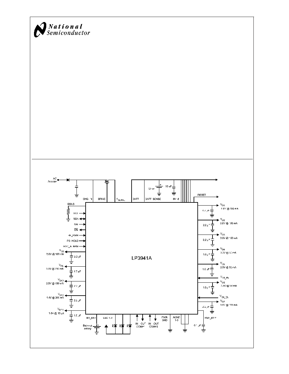
Typical Application
20094501
May 2004
LP3941A
Cellular
Phone
Power
Management
Unit
© 2004 National Semiconductor Corporation
DS200945
www.national.com

Connection Diagrams and Package Mark Information
48-Pin Leadless Leadframe Package
See NS Package Number LQA48B
20094503
Note: Circle marks pin 1 position. Pin 1 name is N/C.
Top View
20094502
Bottom View
20094517
Note: The actual physical placement of the package marking will vary from part to part. The package markings "UZYY" designate assembly and manufacturing
information. "TT" is a NSC internal code for die traceability. Both will vary considerably. "3941LQA" identifies the device.
Package Mark -- Top View
Ordering Information
Order Number
Package Marking
Supplied As
LP3941LQ-A
LP3941LQA
250 units, Tape-and-Reel
LP3941LQX-A
LP3941LQA
2500 units, Tape-and-Reel
Note: *See LP3941A register table and LDO programming table for information on the default voltages for LP3941A.
LP3941A
www.national.com
2
Pin Description
Pin #
Name
I/O
Type
Description
1
N/C
-
-
Not used. Connect to ground.
2
AGND3
G
G
Analog ground pin.
3
V
O8
O
A
LDO 8 Output
4
IN5
I
P
Input power terminal to LDO's. Must be connected to IN14 and IN6.
5
V
O9
O
A
LDO 9 output.
6
V
O10
O
A
LDO 10 output.
7
IN6
I
P
Input power terminal to LDO's. Must be connected to IN15.
8
V
O11
O
A
LDO 11 output.
9
DGND
G
G
Ground pin.
10
V
O3
O
A
LDO 3 output.
11
IN2
I
P
Input power terminal to LDO's. Must be connected to IN1 and IN36.
12
V
O2
O
A
LDO 2 output.
13
IN1
I
P
Input power terminal to LDO's. Must be connected to IN26.
14
V
O1
O
A
LDO 1 output.
15
PS-HOLD
I
D
Active low off key initiated by the micro controller.
16
BU_BAT
I
A
Back-up battery connection.
17
VRTC
O
A
RTC_LDO output.
18
IN (COMP1)
I
A
Non-inverting inout of the comparator 1.
19
OUT (COMP1)
O
A
Output of the comparator 1.
20
AGND1
G
G
Analog ground pin.
21
IN (COMP2)
I
A
Non-inverting input of the comparator 2.
22
OUT (COMP2)
O
A
Output of the comparator 2.
23
REF-BYP
I
A
Reference bypass capacitor.
24
V
O7
O
A
LDO 7 output.
25
V
O6
-EN
I
D
LDO 6 on/off pin. Internal pull-down resistor of 1 M
.
26
IN4
I
P
Input power terminal to LDO's. Must be connected to IN13 and IN56.
27
V
O6
O
A
LDO 6 output.
28
V
O5
O
A
LDO 5 output.
29
IN3
I
P
Input power terminal to LDO's. Must be connected to IN12 and IN46.
30
V
O4
O
A
LDO 4 output.
31
BSNS
I
A
Main battery ID resistor connection.
32
ON
O
OD
Inverted open drain output signal of the ON input. Pulled low when ON is
pulled high and open drain when ON is pulled low. There is no significant
delay between the ON signal going high and ON pin going low. The delay
between ON signal going low and ON pin is determined by the pull up current
and capacitance connected to this pin.
33
BATT
SENSE
I
A
Battery voltage sense pin. Should be connected as close to the battery's +
terminal as possible.
34
Drive
O
A
Gate drive to the external MOSFET.
35
BATT
O
A
Battery supply input terminal. Must have 10 µF ceramic capacitor to GND.
36
V
O5
-EN
I
D
LDO 5 on/off pin. Internal pull down resistor of 1 M
.
37
RTC_ALARM
I
D
RTC_ALARM input.
38
ON
I
D
Active high power On/Off key. This pin is pulled to GND by an internal 200
k
resistor.
39
HF_PWR
I
D
Active high Hands Free connection signal. This pin has an internal 200 k
pull down resistor.
40
CHG_IN
I
P
Charger input from a current limited power source. Must have a 1 µF ceramic
capacitor to GND.
41
I
SENSE
O
A
Charge current sense resistor.
42
RESET
O
OD
Reset output. Active low. (See Power Up Timing Diagram.)
LP3941A
www.national.com
3
Pin Description
(Continued)
Pin #
Name
I/O
Type
Description
43
AGND2
G
G
Analog ground pin.
44
SCL
I
D
Serial interface clock input.
45
SDA
I/O
D
Serial interface data input/output.
46
LED1
O
OD
LED driver output pin.
47
LED2
O
OD
LED driver output pin.
48
LED3
O
OD
LED driver output pin.
A: Analog Pin
D: Digital Pin
G: Ground Pin
P: Power Pin
I: Input Pin
I/O: Input/Output Pin
O: Output Pin
OD: Open Drain Pin
LP3941A
www.national.com
4
Absolute Maximum Ratings
(Notes 1,
2)
If Military/Aerospace specified devices are required,
please contact the National Semiconductor Sales Office/
Distributors for availability and specifications.
CHG-IN
-0.3V to +12V
IN16, BATT, SDA, SCL, ON,
HF-PWR, PS-HOLD, SYS,
COMP1_IN, COMP2_IN,
CHG_IN, BSNS, V
O5
-EN,
V
O6
-EN, LED13,
RTC_ALARM, BU_BAT, V
RTC
,
RESET, BATT
SENSE
.
-0.3V to +6V
REFBYP, ON, PS-HOLD,
COMP1_OUT, COMP2_OUT
to GND
-0.3V to +V
BAT
+ 0.3V
V
O1
to GND
-0.3V to +V
IN1
+ 0.3V
V
O2
, V
O3
to GND
-0.3V to +V
IN2
+ 0.3V
V
O4
, V
O5
to GND
-0.3V to +V
IN3
+ 0.3V
V
O6
, V
O7
to GND
-0.3V to +V
IN4
+ 0.3V
V
O8
, V
O9
to GND
-0.3V to +V
IN5
+ 0.3V
V
O10
, V
O11
to GND
-0.3V to +V
IN6
+ 0.3V
GND to GND SLUG
±
0.3V
Maximum Continuous Power Dissipation
(P
D_MAX
) (Note 3)
3.07W
Junction Temperature (T
J-MAX
)
150°C
Storage Temperature Range
-65°C to +150°C
Maximum Lead Temperature
(Soldering)
(Note 4)
ESD Ratings (Note 5)
All Pins
2 kV HBM
200V MM
Operating Ratings
(Notes 1, 2)
V
IN
3.0V to 6.0V
V
EN
0V to (V
IN
+ 0.3V)
Junction Temperature (T
J
) Range
-40°C to +125°C
Ambient Temperature (T
A
) Range
(Note 6)
-40°C to +85°C
Thermal Properties
(Note 7)
Junction-to-Ambient Thermal
Resistance (
JA
)
26°C/W
Electrical Characteristics
Unless otherwise noted, V
IN
= 2.5V to 5.5V, C
IN
(IN16) = 4.7 µF, C
OUT
(V
O1
and V
O9
) = 4.7 µF, C
OUT
(V
O2
, V
O3
, V
O7
, V
O8
,
V
O10
and V
O11
) = 2.2 µF, C
OUT
(V
O4
to V
O6
) = 1 µF, C
OUT
(V
RTC
) = 1 µF ceramic, C
BYP
= 0.1 µF. Typical values and limits
appearing in normal type apply for T
J
= 25°C. Limits appearing in boldface type apply over the entire junction temperature
range for operation, -40 to +125°C. (Notes 2, 8, 9, 10)
Symbol
Parameter
Condition
Min
Typ
Max
Units
I
Q
Shutdown Supply Current
V
BATT
= 2.1V, UVLO on, internal
logic generator on, V
RTC
off, all other
circuits off.
14
µA
No Load Supply Current, LDO
1 & 3 & 5 on
V
BATT
= 3.6V, LDOs V
O1
, V
O3
and
V
O5
on, back-up battery charger and
V
RTC
on, charger disconnected,
comparator 1 & 2 on.
310
µA
No Load Supply Current
V
BATT
= 3.6V, All LDOs on, charger
disconnected.
500
µA
BATTERY UNDER VOLTAGE LOCKOUT
V
UVLO-R
Under Voltage Lock-Out
V
BATT
Rising
2.91
3.1
3.32
V
V
UVLO-F
Under Voltage Lock-Out
V
BATT
Falling
2.15
2.49
2.85
V
V
TH-POR
Power-On Reset Threshold
V
BATT
Falling Edge
1
1.7
2.3
V
THERMAL SHUTDOWN
Threshold
Hysteresis
160
10
°C
OUTPUT CAPACITORS
C
OUT
Capacitance
ESR
1
5
20
500
µF
m
LOGIC AND CONTROL INPUTS
V
IL
Input Low Level
PS-HOLD, ON, BSNS, HF-PWR,
RTC_ALARM, SDA, SCL, V
O5
-EN,
V
O6
-EN.
2.5V
V
BATT
5.5V
0.4
V
LP3941A
www.national.com
5
Document Outline