LP3942
The Dual RGB LED Controller with 1.5x/2x Charge Pump
and SPI Interface
General Description
The LP3942 is an integrated stand-alone RGB LED control-
ler with a high efficiency and low noise programmable 1.5x
and 2x charge pump. The RGB LEDs are controlled through
the low voltage SPI interface. RGB programmability allows
unique color and brightness control with both RGB outputs.
The color control has preselected color settings for color
blending. The LED current control is done using constant
current sinks that can be also used as switches. The non-
overlapping RGB output PWM control minimizes the input
noise.
See also: LP3931, LP3933 and LP3936 Lighting Manage-
ment Units
Features
n
Pre-regulated 1.5x and 2x charge pump with regulated
output (4.5V and 5.0V)
n
2 separately controlled PWM RGB LED drivers with
programmable color and brightness
n
Overlapping and non-overlapping RGB mode
n
Wide input voltage range 3V≠5.0V
n
Output current up to 120 mA
n
Low voltage SPI interface
n
Programmable low current Standby mode
n
Tiny LLP24 package (5mm*4mm*0.8mm)
Applications
n
Cellular Phones, PDAs
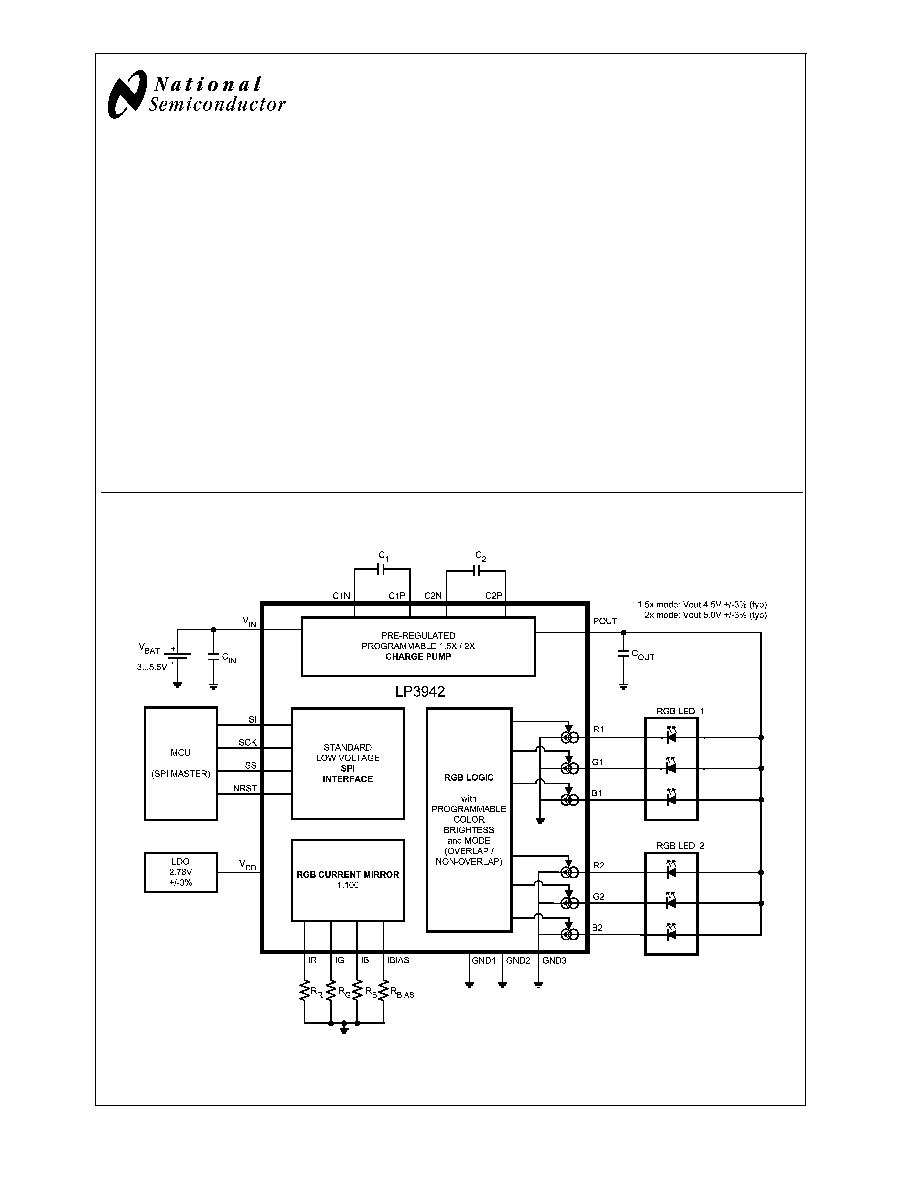
Typical Application
20129201
PRELIMINARY
November 2004
LP3942
The
Dual
RGB
LED
Controller
with
1.5x/2x
Charge
Pump
and
SPI
Interface
© 2004 National Semiconductor Corporation
DS201292
www.national.com
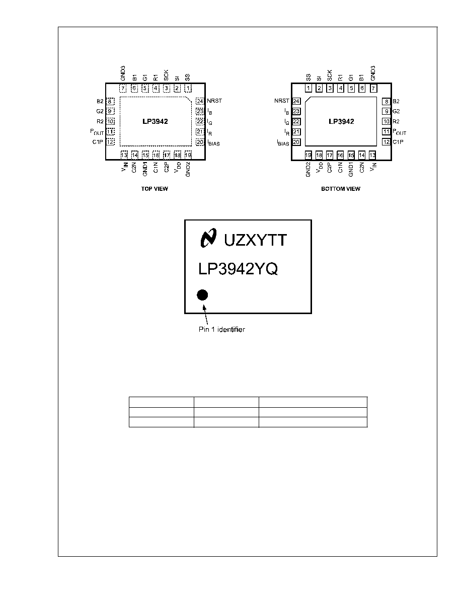
Connection Diagrams and Package Mark Information
24-Lead LLP package (5 mm*4 mm*0.8 mm), Bumped
See NS Package Number YQA24A
20129202
Top View
20129203
Bottom View
20129204
Package Mark -- Top View
Note: The actual physical placement of the package marking will vary from part to part. The package marking "XY" designates the date code. "UZ" and "TT" are NSC
internal codes for die manufacturing and assembly traceability. Both will vary considerably.
Ordering Information
Order Number
Package Marking
Supplied As
LP3942YQ
LP3942YQ
1000 units, Tape-and-Reel
LP3942YQX
LP3942YQX
2500 units, Tape-and-Reel
LP3942
www.national.com
2
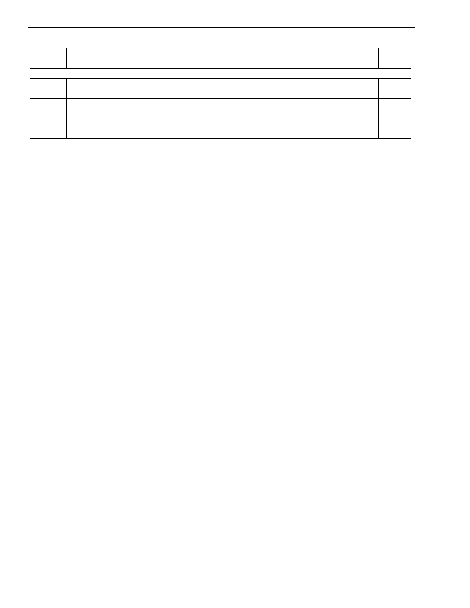
Pin Description
Pin #
Name
Type
Description
1
SS
Logic Input
SPI Slave Select
2
SI
Logic Input
SPI Serial Data
3
SCK
Logic Input
SPI Clock
4
R1
Output
Open Drain, Red LED (1)
5
G1
Output
Open Drain, Green LED (1)
6
B1
Output
Open Drain, Blue LED (1)
7
GND3
Ground
Ground 3
8
B2
Output
Open Drain, Blue LED (2)
9
G2
Output
Open Drain, Green LED (2)
10
R2
Output
Open Drain, Red LED (2)
11
P
OUT
Output
Charge Pump Output
12
C1P
Flying capacitor C1 connection
13
V
IN
Power
Input voltage from battery
14
C2N
Flying capacitor C2 connection
15
GND1
Ground
Ground 1
16
C1N
Flying capacitor C1 connection
17
C2P
Flying capacitor C2 connection
18
V
DD
Power
LDO/Supply voltage input
19
GND2
Ground
Ground 2
20
I
BIAS
Input
Bias resistor connection
21
I
R
Input
Red LED current set resistor
22
I
G
Input
Green LED current set resistor
23
I
B
Input
Blue LED current set resistor
24
NRST
Logic Input
Low active reset input pin. (Internal pull down 1 M
)
LP3942
www.national.com
3
Absolute Maximum Ratings
(Notes 1,
2)
If Military/Aerospace specified devices are required,
please contact the National Semiconductor Sales Office/
Distributors for availability and specifications.
V
IN
Pin: Voltage to GND
-0.3V to +6.0V
Voltage on R1, G1, B1, R2, G2,
B2 Pins
-0.3V to P
OUT
+ 0.3V, with 6.0V max
Voltage on All Other Pins
-0.3V to V
IN
+0.3V,
with 6.0V max
Continuous Power Dissipation
(Note 3)
Internally Limited
Junction Temperature (T
J-MAX
)
150∞C
Storage Temperature Range
-65∞C to +150∞C
Maximum Lead Temperature
(Soldering)
(Note 4)
ESD Rating (Note 5)
Human Body Model:
2.0 kV
Machine Model:
200V
Operating Ratings
(Notes 1, 2)
Input Voltage Range
3.0V to 5.0V
V
DD
Voltage Range
2.69V to 2.87V
Recommended Load Current
0 mA to 120 mA
Junction Temperature (T
J
) Range
-30∞C to +105∞C
Ambient Temperature (T
A
) Range
(Note 6)
-30∞C to +85∞C
Thermal Properties
Junction-to-Ambient Thermal Resistance
A
34∞C/W
(
JA
), LLP24 Package (Notes 6, 7)
Electrical Characteristics
(Notes 2, 8)
Limits in standard typeface are for T
J
= +25∞C. Limits in boldface type apply over the operating junction temperature range
(-30∞C
T
A
+105∞C). Unless otherwise noted, specifications apply to the LP3942 Typical Application Circuit (pg. 1) with:
V
VDD
= 2.78V, V
IN
3.6V, C
IN
= 2.2 µF, C
1
= 1.0 µF, C
2
= 1.0 µF, C
OUT
= 3.0 µF, R
BIAS
= 27k. (Note 9).
Symbol
Parameter
Condition
Min
Typ
Max
Units
CHARGE PUMP 1.5x MODE
V
POUT
Output Voltage
3.4V
<
V
IN
<
5.0V,
I
OUT
120 mA
4.5
V
3.0V
<
V
IN
<
3.4V
(1.5xV
IN
)
≠ (I
OUT
x
R
OUT
)
Accuracy (Note 10)
3.4V
<
V
IN
<
5.0V,
I
OUT
120 mA
±
3
±
5
%
R
OUT
Output Resistance
V
DD
= 3.0V
5
7
G
CP
Charge Pump Gain
1.5
CHARGE PUMP 2x MODE
V
POUT
Output Voltage (Note 10)
3.20V
<
V
IN
<
5.0V,
I
OUT
120 mA
4.75
5.0
±
3
5.25
±
5
V
%
3.0V
<
V
IN
<
3.2V,
I
OUT
80 mA
4.75
5.0
±
3
5.25
±
5
V
%
R
OUT
Output Resistance
V
DD
= 3.0V
5
G
CP
Charge Pump Gain
2
Symbol
Parameter
Condition
Min
Typ
Max
Units
I
Q
(V
IN
)
Operating Quiescent Current
I
(OUT)
= 0A (Note 11)
1.0
3.0
mA
I
Q
(V
DD
)
Operating Quiescent Current
200
300
µA
I
SD
(V
IN
)
Standby Quiescent Current
NSTBY = 0
NRST pin current excluded
4
10
µA
I
SD
(V
DD
)
Standby Quiescent Current
NSTBY = 0,
SPI interface inputs at 0V or 1.8V
NRST pin current excluded
0.5
2
µA
f
sw
Switching Frequency
R
BIAS
= 27 k
±
1%
500
625
750
kHz
t
start
Startup Time
After writing `1' to NSTBY AND
CP_ON. NRST must be `1'.
1
2
ms
T
SHD
Shutdown Threshold.
Hysteresis
160
20
∞C
∞C
LP3942
www.national.com
4
Logic Interface Characteristics (1.8V Logic)
Symbol
Parameter
Conditions
Limit
Units
Min
Typ
Max
LOGIC INPUTS
V
IL
Input Low Level
SS, SI, SCK, NRST
0.5
V
V
IH
Input High Level
SS, SI, SCK, NRST
1.2
V
I
H
Logic Input Current
SS, SI, SCK
NRST (1 M
pull-down)
-1
-1
1
3
µA
µA
f
SPI
Interface Clock
10
MHz
t
NRST
Reset Pulse Width
NRST
50
µs
Note 1: Absolute Maximum Ratings indicate limits beyond which damage to the component may occur. Operating Ratings are conditions under which operation of
the device is guaranteed. Operating Ratings do not imply guaranteed performance limits. For guaranteed performance limits and associated test conditions, see the
Electrical Characteristics tables.
Note 2: All voltages are with respect to the potential at the GND pins.
Note 3: Internal thermal shutdown circuitry protects the device from permanent damage. Thermal shutdown engages at T
J
= 160∞C (typ.) and disengages at T
J
=
140∞C (typ.).
Note 4: For detailed soldering specifications and information, please refer to National Semiconductor Application Note 1187: Leadless Leadframe
Package (LLP).
Note 5: The Human body model is a 100 pF capacitor discharged through a 1.5 k
resistor into each pin. The machine model is a 200 pF capacitor discharged
directly into each pin. MIL-STD-883 3015.7
Note 6: In applications where high power dissipation and/or poor package thermal resistance is present, the maximum ambient temperature may have to be
derated. Maximum ambient temperature (T
A-MAX
) is dependent on the maximum operating junction temperature (T
J-MAX-OP
= 105∞C), the maximum power
dissipation of the device in the application (P
D-MAX
), and the junction-to ambient thermal resistance of the part/package in the application (
JA
), as given by the
following equation: T
A-MAX
= T
J-MAX-OP
- (
JA
x P
D-MAX
).
Note 7: Junction-to-ambient thermal resistance (
JA
) is taken from a thermal modeling result, performed under the conditions and guidelines set forth in the JEDEC
standard JESD51-7. The test board is a 4-layer FR-4 board measuring 102 mm x 76 mm x 1.6 mm with a 2x1 array of thermal vias. The ground plane on the board
is 50 mm x 50 mm. Thickness of copper layers are 36 µm/18 µm/18 µm/36 µm (1.5 oz/1 oz/1 oz/1.5 oz). Ambient temperature in simulation is 22∞C, still air. Power
dissipation is 1W.
The value of
JA
of the LP3942 in LLP-24 could vary widely, depending on PWB material, layout, and environmental conditions. In applications where high maximum
power dissipation exists (high V
IN
, high I
OUT
), special care must be paid to thermal dissipation issues. For more information on these topics, please refer to
Application Note 1187: Leadless Leadframe Package (LLP) and the Power Efficiency and Power Dissipation section of this datasheet.
Note 8: Min and Max limits are guaranteed by design, test, or statistical analysis. Typical numbers are not guaranteed, but do represent the most likely norm.
Note 9: C
IN
, C
OUT
, C1, and C2 : Low-ESR Surface-Mount Ceramic Capacitors (MLCCs) used in setting electrical characteristics. Minimum capacitance value for
C
IN
, C
1
, and C
2
capacitors is 70% of nominal value. This tolerance includes manufacturing tolerance, temperature coefficient and voltage dependency (roll-off). C
OUT
minimum effective capacitance value is 3.0 µF.
Note 10: Output voltage accuracy does not include V
DD
(2.78V supply voltage) tolerance.
Note 11: The quiescent current does not include the current setting resistors' current.
LP3942
www.national.com
5