 | ÐлекÑÑоннÑй компоненÑ: LP3943ISQ | СкаÑаÑÑ:  PDF PDF  ZIP ZIP |
Äîêóìåíòàöèÿ è îïèñàíèÿ www.docs.chipfind.ru
LP3943
RGB/White/Blue 16-LED Fun Light Driver
General Description
LP3943 is an integrated device capable of independently
driving 16 LEDs. This device also contains an internal pre-
cision oscillator that provides all the necessary timing re-
quired for driving each LED. Two prescaler registers along
with two PWM registers provide a versatile duty cycle con-
trol. The LP3943 contains the ability to dim LEDs in SMBUS/
I
2
C applications where it is required to cut down on bus
traffic.
Traditionally, to dim LEDs using a serial shift register such as
74LS594/5 would require a large amount of traffic to be on
the serial bus. LP3943 instead requires only the setup of the
frequency and duty cycle for each output pin. From then on,
only a single command from the host is required to turn each
individual open drain output ON, OFF, or to cycle a pro-
grammed frequency and duty cycle. Maximum output sink
current is 25 mA per pin and 200 mA per package. Any ports
not used for controlling the LEDs can be used for general
purpose input/output expansion.
Features
n
Internal power-on reset
n
Active low reset
n
Internal precision oscillator
n
Variable dim rates (from 6.25 ms to 1.6s;
160 Hz0.625 Hz)
Key Specifications
n
16 LED driver (multiple programmable states -- on, off,
input, and dimming at a specified rate)
n
16 Open drain outputs capable of driving up to 25 mA
per LED
Applications
n
Customized flashing LED lights for cellular phones
n
Portable Applications
n
Digital Cameras
n
Indicator Lamps
n
General purpose I/O expander
n
Toys
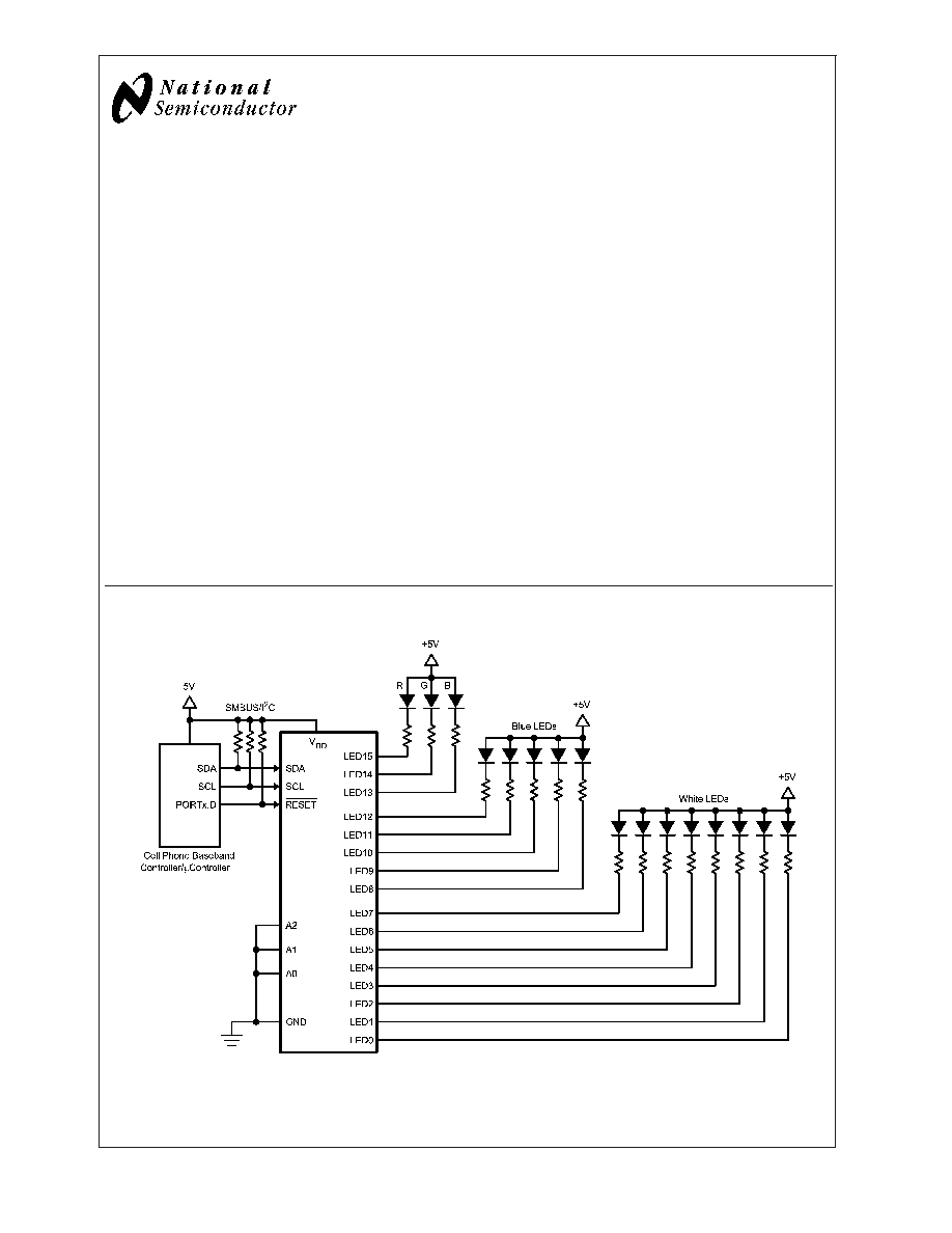
Typical Application Circuit
20079601
November 2003
LP3943
RGB/White/Blue
16-LED
Fun
Light
Driver
© 2003 National Semiconductor Corporation
DS200796
www.national.com
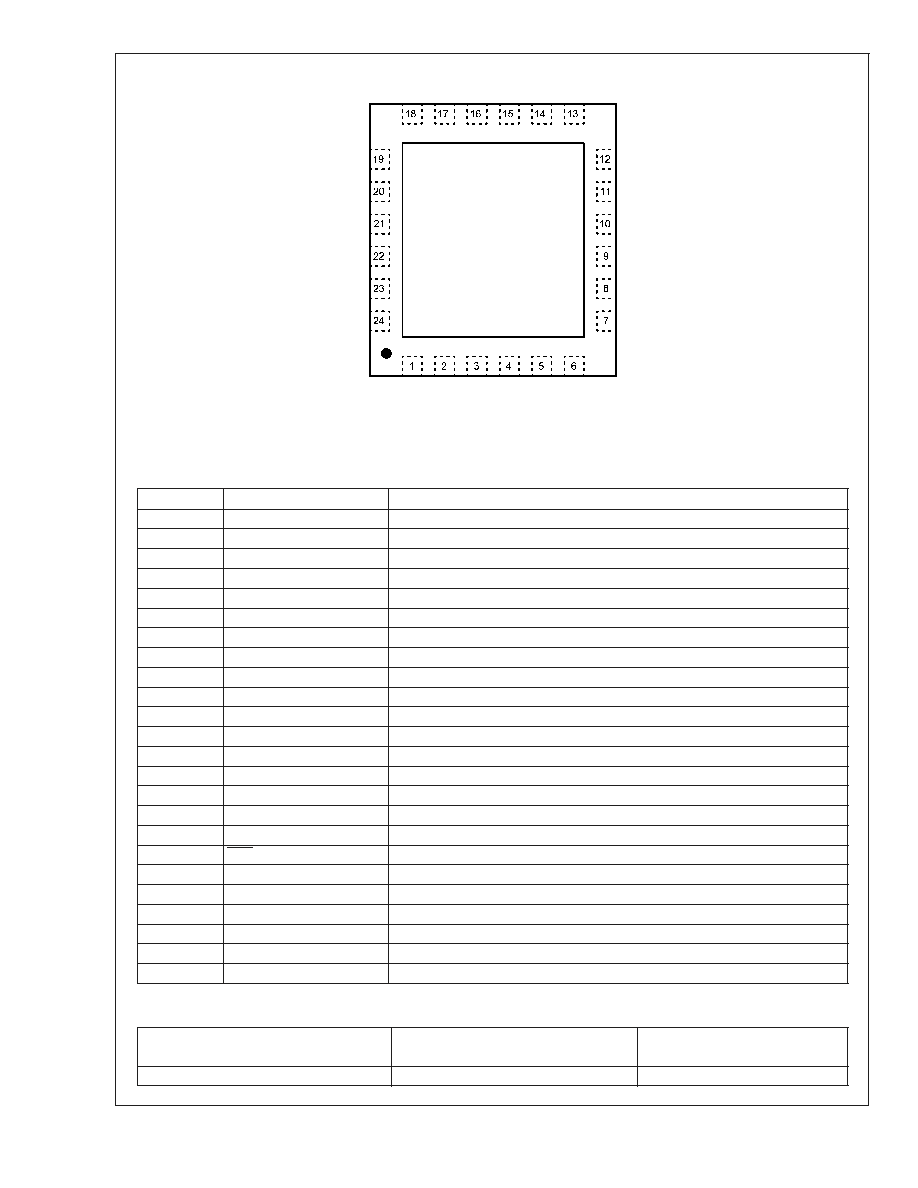
LP3943 Pin Out
20079602
(Top View)
See NS Package Number SQA24C
LP3943 Pin Description
Pin #
Name
Description
1
LED0
Output of LED0 Driver
2
LED1
Output of LED1 Driver
3
LED2
Output of LED2 Driver
4
LED3
Output of LED3 Driver
5
LED4
Output of LED4 Driver
6
LED5
Output of LED5 Driver
7
LED6
Output of LED6 Driver
8
LED7
Output of LED7 Driver
9
GND
Ground
10
LED8
Output of LED8 Driver
11
LED9
Output of LED9 Driver
12
LED10
Output of LED10 Driver
13
LED11
Output of LED11 Driver
14
LED12
Output of LED12 Driver
15
LED13
Output of LED13 Driver
16
LED14
Output of LED14 Driver
17
LED15
Output of LED15 Driver
18
RST
Active Low Reset Input
19
SCL
Clock Line for I
2
C Interface
20
SDA
Serial Data Line for I
2
C Interface
21
V
DD
Power Supply
22
A0
Address Input 0
23
A1
Address Input 1
24
A2
Address Input 2
Ordering Information
LP3943, Supplied as 1000 Units, Tape and
Reel
LP3943, Supplied as 4500 Units, Tape
and Reel
Package Marking
LP3943ISQ
LP3943ISQX
LP3943
LP3943
www.national.com
2
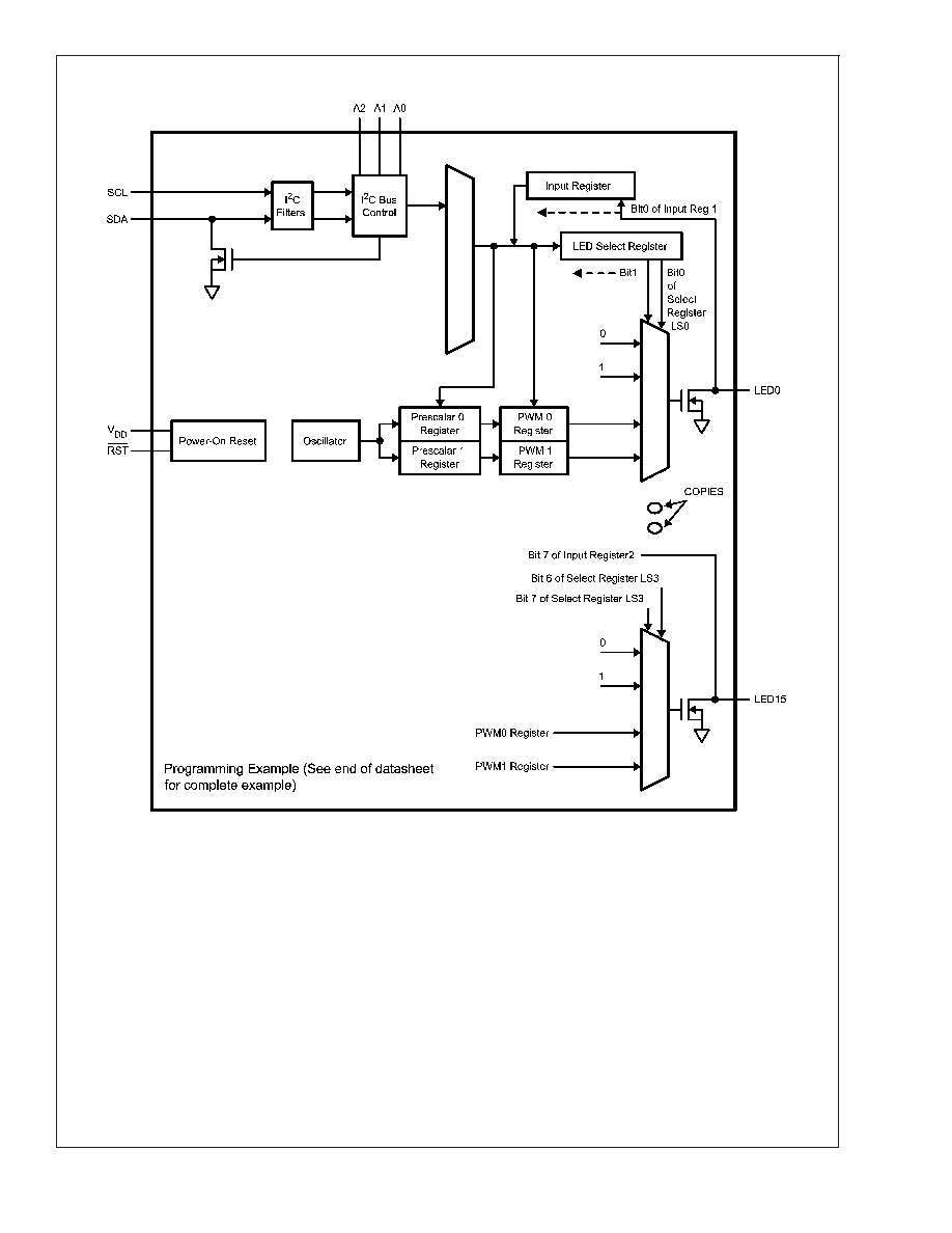
Architectural Block Diagram
20079603
For Explanation of LP3943 Operation, Please Refer to "Theory of Operation" in Application Notes.
LP3943
www.national.com
3
Absolute Maximum Ratings
(Notes 2,
1)
If Military/Aerospace specified devices are required,
please contact the National Semiconductor Sales Office/
Distributors for availability and specifications.
V
DD
-0.5V to 6V
A0, A1, A2, SCL, SDA, RST
(Collectively called digital pins)
6V
Voltage on LED pins
V
SS
-0.5V to 6V
Junction Temperature
150°C
Storage Temperature
-65°C to 150°C
Power Dissipation (Note 3)
400 mW
ESD (Note 4)
Human Body Model
2 kV
Machine Model
200V
Charge Device Model
1 kV
Operating Ratings
(Notes 1, 2)
V
DD
2.3V to 5.5V
Junction Temperature
-40°C to +125°C
Operating Ambient Temperature
-40°C to +85°C
Thermal Resistance (
JA
)
LLP24 (Note 3)
37°C/W
Electrical Characteristics
Unless otherwise noted, V
DD
= 5.5V. Typical values and limits appearing in normal type apply for T
J
= 25°C. Limits appearing
in boldface type apply over the entire junction temperature range for operation, T
J
= -40°C to +125°C. (Note 5)
Symbol
Parameter
Conditions
Typical
Limit
Units
Min
Max
POWER SUPPLY
V
DD
Supply Voltage
5
2.3
5.5
V
I
Q
Supply Current
No Load
350
550
µA
Standby
2.0
5
I
Q
Additional Standby Current
V
DD
= 5.5V, every LED pin
at 4.3V
2
mA
V
POR
Power-On Reset Voltage
1.8
1.96
V
t
w
Reset Pulse Width
10
ns
LED
V
IL
LOW Level Input Voltage
-0.5
0.8
V
V
IH
HIGH Level Input Voltage
2.0
5.5
V
I
OL
Low Level Output Current
(Note 6)
V
OL
= 0.4V, V
DD
= 2.3V
9
mA
V
OL
= 0.4V, V
DD
= 3.0V
12
V
OL
= 0.4V, V
DD
= 5.0V
15
V
OL
= 0.7V, V
DD
= 2.3V
15
V
OL
= 0.7V, V
DD
= 3.0V
20
V
OL
= 0.7V, V
DD
= 5.0V
25
I
LEAK
Input Leakage Current
V
DD
= 3.6, V
IN
= 0V or V
DD
-1
1
µA
C
I/O
Input/Output Capacitance
(Note 7)
2.6
5
pF
ALL DIGITAL PINS (EXCEPT SCL AND SDA PINS)
V
IL
LOW Level Input Voltage
-0.5
0.8
V
V
IH
HIGH Level Input Voltage
2.0
5.5
V
I
LEAK
Input Leakage Current
-1
1
µA
C
IN
Input Capacitance
V
IN
= 0V (Note 7)
2.3
5
pF
I
2
C INTERFACE (SCL AND SDA PINS)
V
IL
LOW Level Input Voltage
-0.5
0.3V
DD
V
V
IH
HIGH Level Input Voltage
0.7V
DD
5.5
V
V
OL
LOW Level Output Voltage
0
0.2V
DD
V
I
OL
LOW Level Output Current
V
OL
= 0.4V
6.5
3
mA
F
CLK
Clock Frequency
(Note 7)
400
kHz
t
HOLD
Hold Time Repeated START
Condition
(Note 7)
0.6
µs
t
CLK-LP
CLK Low Period
(Note 7)
1.3
µs
LP3943
www.national.com
4
Electrical Characteristics
(Continued)
Unless otherwise noted, V
DD
= 5.5V. Typical values and limits appearing in normal type apply for T
J
= 25°C. Limits appearing
in boldface type apply over the entire junction temperature range for operation, T
J
= -40°C to +125°C. (Note 5)
Symbol
Parameter
Conditions
Typical
Limit
Units
Min
Max
I
2
C INTERFACE (SCL AND SDA PINS)
t
CLK-HP
CLK High Period
(Note 7)
0.6
µs
t
SU
Set-Up Time Repeated
START Condition
(Note 7)
0.6
µs
t
DATA-HOLD
Data Hold Time
(Note 7)
300
ns
t
DATA-SU
Data Set-Up Time
(Note 7)
100
ns
t
SU
Set-Up Time for STOP
Condition
(Note 7)
0.6
µs
t
TRANS
Maximum Pulse Width of
Spikes that Must Be
Suppressed by the Input
Filter of Both DATA & CLK
Signals
(Note 7)
50
ns
Note 1: Absolute Maximum Ratings are limits beyond which damage to the device may occur. Operating Ratings are conditions under which operation of the device
is guaranteed. Operating Ratings do not imply guaranteed performance limits. For guaranteed performance limits and associated test conditions, see the Electrical
Characteristics tables.
Note 2: All voltages are with respect to the potential at the GND pin.
Note 3: The part cannot dissipate more than 400mW.
Note 4: The human-body model is 100 pF discharged through 1.5 k
. The machine model is 0 in series with 100 pF.
Note 5: Limits are guaranteed. All electrical characteristics having room-temperature limits are tested during production with T
J
= 25°C. All hot and cold limits are
guaranteed by correlating the electrical characteristics to process and temperature variations and applying statistical process control.
Note 6: Each LED pin should not exceed 25 mA and each octal (LED0LED7; LED8LED15) should not exceed 100 mA. The package should not exceed a total
of 200 mA.
Note 7: Guaranteed by design.
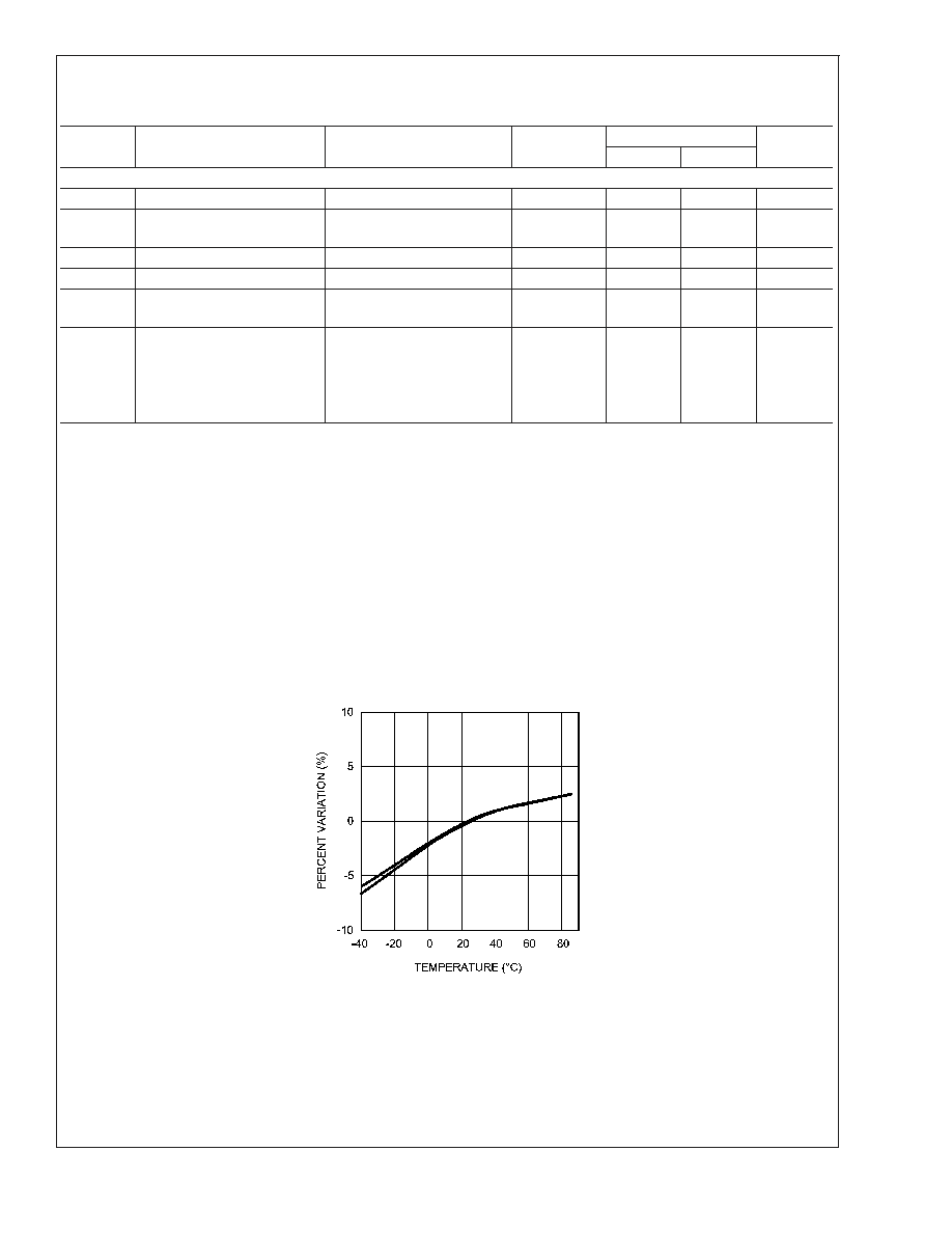
Typical Performance Characteristics
Frequency vs. Temp
(T
A
= -40°C to +85°C),
V
DD
= 2.3V to 3.0V
20079617
LP3943
www.national.com
5
Document Outline