LP3945/LP3946
Battery Charge Management System
General Description
The LP3945 and LP3946 are complete charge management
systems that safely charge and maintain a Li-Ion battery or a
four-cell Ni-MH (LP3945 only) battery pack. The LP3945
offers the flexibility of programming charge current, battery
regulation voltage (4.1V/4.2V), battery type (Li-Ion/Ni-MH),
and End Of Charge (EOC) termination through the use of I
2
C
interface. On the LP3946, these parameters are pro-
grammed at the factory per customer specification.
The pass transistor, charge current sensing resistor and
charge current setting resistors are all integrated inside the
LP3945 and LP3946. This eliminates the use of external
components and significantly reduces design time and board
space.
The LP3945 and LP3946 operate in four modes: pre-
qualification, constant current, constant voltage and mainte-
nance modes. The LP3945 features Ni-MH charging mode
as well. The charger has under-voltage and over-voltage
protection as well as an internal 5.6 hr timer to prevent
overcharging the battery. There are two open drain outputs
for status indication. An internal amplifier readily converts the
charge current into a voltage. Also, the charger can operate
in an LDO mode providing up to 1 Amp to the load.
Features
n
Integrated pass transistor
n
Does not require external charge current setting or
sensing resistors
n
I
2
C interface (LP3945 only) -- programmable charge
current, EOC current and battery regulation voltage
n
Near-depleted battery preconditioning
n
Built-in 5.6 hour timer
n
Under voltage and over voltage lockout on adaptor
n
Charge status indicators
n
Charge current monitor analog output
n
LDO mode operation can source 1 amp
n
Continuous over current/temperature protection
Key Specifications
n
1% charger voltage accuracy over 0∞C
T
J
85∞C
n
4.5V to 6.0V input voltage range
n
LLP package power dissipation: 2.7W at T
A
= 25∞C
Applications
n
Cellular phones
n
PDAs
n
Digital cameras
n
USB powered devices
n
Programmable current sources
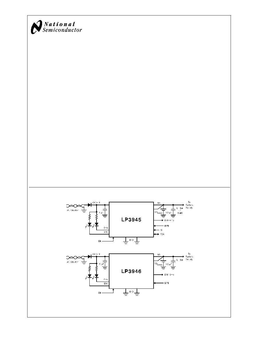
Typical Application Circuit
20066502
20066501
October 2003
LP3945/LP3946
Battery
Charge
Management
System
© 2003 National Semiconductor Corporation
DS200665
www.national.com
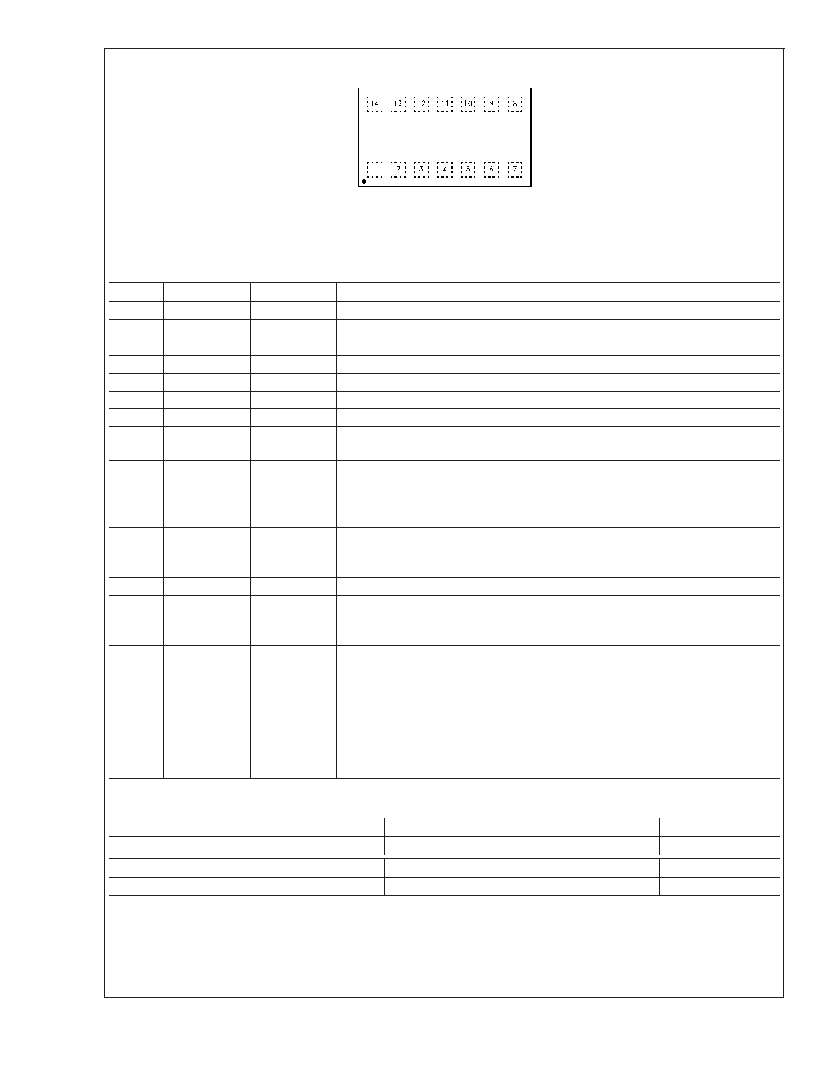
LP3945/LP3946 LLP14 Package Drawing
20066503
(TOP VIEW)
See NS Package Number LDA14A
LP3945/LP3946 Pin Description
Pin #
LP3945
LP3946
Description
1
EN
EN
Charger Enable Input. Internally pulled high to CHG-IN pin.
2
SCL
GND
Serial Interface Clock Input for LP3945. Ground in LP3946.
3
SDA
GND
Serial Interface DATA Input/Output for LP3945. Ground in LP3946.
4
BATT
BATT
Battery supply input terminal. Must have 10 µF ceramic capacitor to GND.
5
V
BG
V
BG
Bandgap Voltage Reference (1.225V). Factory test point. Must be left floating.
6
VB
SENSE
VB
SENSE
Battery Voltage Sense connected to the + terminal of the battery.
7
GND
GND
Digital Ground
8
Diff-Amp
Diff-Amp
Charge current monitoring differential amplifier output. Voltage output representation
of the charge current.
9
BIPB
BIPB
Battery in Place Bar. Input signal to indicate presence/absence of the battery.
Internally pulled high to CHG-IN. Pulled low by the Battery ID resistor. Absence of
the ID resistor (BIPB signal high) indicates no battery. Pulling BIPB pin high sets the
device to LDO mode.
10
EOC
EOC
Active Low Open Drain Output to drive Green LED. Active when wall adaptor is
connected and battery is fully charged. Regardless of the battery chemistry, this
signal is available whenever a battery is attached.
11
GND
GND
Analog Ground
12
CHG
CHG
Active Low Open Drain Output to drive Red LED. Active when wall adaptor is
connected and battery is being charged. Regardless of the battery chemistry, this
signal is available whenever a battery is attached.
13
StopModeEN
StopModeEN
For normal operation, this pin must be left floating. Pulling this pin to ground will
bypass the 5.6 Hrs safety timer in constant current mode. See "StopModeEN PIN"
Section for more detail.
WARNING! Disabling the timer is not a recommended operating condition
since it disables the safety timer function. User must provide protection
against continuously charging a defective battery.
14
CHG-IN
CHG-IN
Charger input from a regulated, current limited power source. Must have a 1 µF
ceramic capacitor to GND.
Ordering Information
LP3945 supplied as 1000 units Tape and Reel
LP3945 supplied as 4500 units Tape and Reel
Package Marking
LP3945ILD
LP3945ILDX
L00011B
LP3946 supplied as 1000 units Tape and Reel
LP3946 supplied as 4500 units Tape and Reel
Package Marking
LP3946ILD
LP3946ILDX
L00030B
The LP3946 has default values of I
CHG
=500mA, V
BATT
=4.1V and EOC=0.1C. For other default options, please contact National
Semiconductor Sales Office.
LP3945/LP3946
www.national.com
2
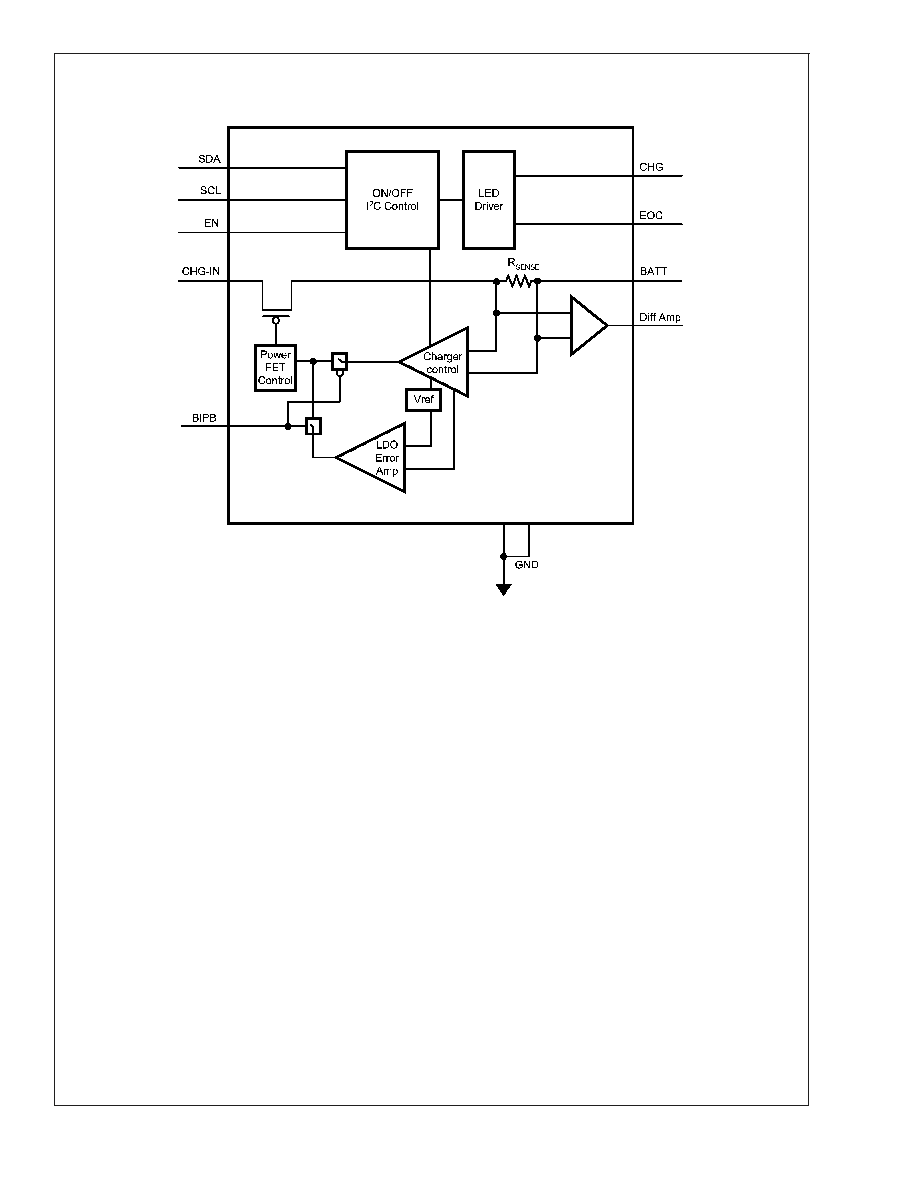
Block Diagram
LP3945 Functional Block Diagram
20066530
LP3945/LP3946
www.national.com
3
Absolute Maximum Ratings
(Notes 1,
2)
If Military/Aerospace specified devices are required,
please contact the National Semiconductor Sales Office/
Distributors for availability and specifications.
CHG-IN
-0.3V to +6.5V
BATT, VB
SENSE
, SDA, SCL, EOC,
CHG, EN, BIPB, StopModeEN
-0.3V to +6V
Junction Temperature
150∞C
Storage Temperature
-65∞C to +150∞C
Power Dissipation (Note 3)
1.76W
ESD (Note 4)
Human Body Model
Machine Model
2kV
200V
Operating Ratings
(Notes 1, 2)
CHG-IN
3.0V to 6.0V
EN, BIPB, StopModeEN
0V to (V
CHG-IN
+0.3V)
Junction Temperature, T
J
-40∞C to +125∞C
Operating Temperature, T
A
-40∞C to +85∞C
Thermal Resistance,
JA
37∞C/W
Maximum Power Dissipation
(T
A
= 85∞C, (Note 5) )
1.08W
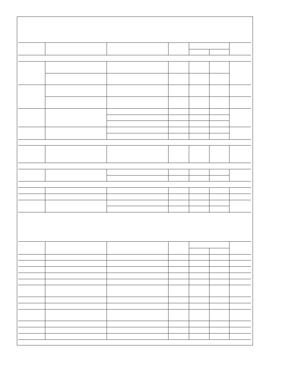
Electrical Characteristics
Unless otherwise noted, V
CHG-IN
= 5V, V
BATT
= 4V, C
CHG-IN
= 1µF, C
BATT
= 10µF. Typical values and limits appearing in nor-
mal type apply for T
J
= 25∞C. Limits appearing in boldface type apply over the entire junction temperature range for operation,
T
J
= -40∞C to +85∞C. (Notes 6, 7, 8)
Symbol
Parameter
Conditions
Typical
Limit
Units
Min
Max
V
CC
SUPPLY
V
CHG-IN
Input Voltage Range
4.5
6
V
Operating Range
Battery Connected
4.5
6
I
BATT
Battery Leakage Current
V
CHG-IN
4V
2
20
µA
EOC = Low, adaptor connected,
V
BATT
= 4.1V
50
150
µA
V
OK-TSHD
Adapter OK Trip Point (CHG-IN)
V
CHG-IN
- V
BATT
(Rising)
60
mV
V
CHG-IN
- V
BATT
(Falling)
50
mV
V
UVLO-TSHD
Under Voltage Lock-out Trip
Point
V
CHG-IN
(Rising)
4.15
3.8
4.5
V
V
CHG-IN
(Falling)
3.95
3.6
4.3
V
V
OVLO-TSHD
Over Voltage Lock-out Trip Point
V
CHG-IN
(Rising)
5.9
V
V
CHG-IN
(Falling)
5.7
Thermal Shutdown Temperature
(Note 7)
160
∞C
Thermal Shutdown Hysteresis
20
∞C
BATTERY CHARGER -- Li ION MODE (MODE = LOW)
I
CHG
Fast Charge Current Range
500
950
mA
Fast Charge Current Accuracy
-10
+10
%
Programmable Charging Current
Step
50
mA
I
PRE-CHG
Pre-Charge Current
V
BATT
= 2V
50
65
mA
I
EOC
End Of Charge Current Accuracy For I
EOC
= 0.1C, 0.15C or 0.2C
+20
-20
%
V
BATT
Battery Regulation Voltage
(For 4.1V Cell) (Default State)
T
J
= 0∞C to +85∞C
I
CHARGE
= 10 mA, Mode = Low
4.1
4.059
4.141
V
T
J
= -40∞C to +85∞C
I
CHARGE
= 10 mA, Mode = Low
4.1
4.038
4.162
Battery Regulation Voltage
(For 4.2V Cell)
T
J
= 0∞C to +85∞C
I
CHARGE
= 10 mA, Mode = Low
4.2
4.158
4.242
T
J
= -40∞C to +85∞C
I
CHARGE
= 10 mA, Mode = Low
4.2
4.137
4.263
V
CHG-Q
Full Charge Qualification
Threshold
V
BATT
Rising, Transition from
Pre-Charge to Full Current
3.0
V
LP3945/LP3946
www.national.com
4
Electrical Characteristics
(Continued)
Unless otherwise noted, V
CHG-IN
= 5V, V
BATT
= 4V, C
CHG-IN
= 1µF, C
BATT
= 10µF. Typical values and limits appearing in nor-
mal type apply for T
J
= 25∞C. Limits appearing in boldface type apply over the entire junction temperature range for operation,
T
J
= -40∞C to +85∞C. (Notes 6, 7, 8)
Symbol
Parameter
Conditions
Typical
Limit
Units
Min
Max
BATTERY CHARGER -- Li ION MODE (MODE = LOW)
V
BAT-RST
Restart Threshold Voltage
(For 4.1V Cell)
V
BATT
Falling, Transition from
EOC, to Pre-Qualification State
3.9
3.77
4.02
V
Restart Threshold Voltage
(For 4.2V Cell)
V
BATT
Falling, Transition from
EOC, to Pre-Qualification State
4.00
3.86
4.12
R
SENSE
Internal Current Sense
Resistance
(Note 7)
120
m
Internal Current Sense Resistor
Load Current
(Note 7)
1.2
A
ICHG
MON
Diff-Amp Output
I
CHG
= 50 mA
0.583
V
I
CHG
= 500 mA
1.333
I
CHG
= 950 mA
2.090
t
EOC
Time to EOC State
0∞C to +85∞C (Note 7)
5.625
4.78
6.42
Hrs
-40∞C to +85∞C (Note 7)
5.625
4.5
6.75
BATTERY CHARGER -- NI-MH MODE (MODE = HIGH, LP3945 ONLY)
V
BATT-MAX
Battery Over Voltage Protection
(Charging Current Decreases to
0 mA when V
BATT
is above this
Voltage), V
CHG-IN
= 5.6V
5.4
5.292
5.508
V
LDO MODE (BIPB=HIGH)
V
OUT
Output Voltage Regulation
I
LOAD
=50mA
4.10
V
I
LOAD
=950mA
4.06
LOGIC LEVELS
V
IL
Low Level Input Voltage
EN
0.4
V
V
IH
High Level Input Voltage
EN
2.0
V
I
IL
Enable Pin Input Current
EN = LOW
-10
+10
µA
EN = HIGH
-5
+5
Electrical Characteristics, I
2
C Interface (LP3945 Only)
Unless otherwise noted, V
CHG-IN
= 5V, V
BATT
= 4V. Typical values and limits appearing in normal type apply for T
J
= 25∞C.
Limits appearing in boldface type apply over the entire junction temperature range for operation, T
J
= -40∞C to +85∞C. (Notes
6, 7, 8)
Symbol
Parameter
Conditions
Typical
Limit
Units
Min
Max
V
IL
Low Level Input Voltage
SDA & SCL
0.4
0.3 V
DD
V
V
IH
High Level Input Voltage
SDA & SCL
0.7 V
DD
V
DD
+0.5
V
V
OL
Low Level Output Voltage
SDA & SCL
0
0.2 V
DD
V
V
HYS
Schmitt Trigger Input Hysteresis
SDA & SCL
0.1 V
DD
V
F
CLK
Clock Frequency
400
kHz
t
HOLD
Hold Time Repeated START
Condition
(Note 7)
0.6
µs
t
CLK-LP
CLK Low Period
(Note 7)
1.3
µs
t
CLK-HP
CLK High Period
(Note 7)
0.6
µs
t
SU
Set-up Time Repeated START
Condition
(Note 7)
0.6
µs
t
DATA-HOLD
Data Hold Time
(Note 7)
300
ns
t
DATA-SU
Data Set-up Time
(Note 7)
100
ns
t
SU
Set-up Time for STOP Condition
(Note 7)
0.6
µs
LP3945/LP3946
www.national.com
5