LP3947
USB/AC Adaptor, Single Cell Li-Ion Battery Charger IC
General Description
The LP3947 is a complete charge management system that
safely charges and maintains a Li-Ion battery from either
USB power source or AC adaptor. In USB mode, the LP3947
supports charging in low power or high power mode. Alter-
natively, the LP3947 can take charge from AC adaptor. In
both USB and AC adaptor modes, charge current, battery
regulation voltage, and End of Charge (EOC) point can be
selected via I
2
C interface. The LP3947 can also operate on
default values that are pre-programmed in the factory. The
battery temperature is monitored continuously at the Ts pin
to safeguard against hazardous charging conditions. The
charger also has under-voltage and over-voltage protection
as well as an internal 5.6 hr timer to protect the battery. The
pass transistor and charge current sensing resistor are all
integrated inside the LP3947.
The LP3947 operates in four modes: pre-qualification, con-
stant current, constant voltage and maintenance modes.
There are two open drain outputs for status indication. An
internal amplifier readily converts the charge current into a
voltage. Also, the charger can operate in an LDO mode
providing a maximum of 1.2 Amp to the load.
Features
n
Supports USB Charging Scheme
n
Integrated Pass Transistor
n
Near-Depleted Battery Preconditioning
n
Monitors Battery Temperature
n
Built-In 5.6 hour timer
n
Under Voltage and Over Voltage Lockout
n
Charge Status Indicators
n
Charge Current Monitor Analog Output
n
LDO Mode Operation can source 1 Amp
n
Continuous Over Current/Temperature Protection
Key Specifications
n
1% Charger Voltage Accuracy Over 0∞C
T
J
85∞C
n
4.3V to 6.0V Input Voltage Range
n
100 mA to 750 mA charge current range, in charger
mode
n
100mA to 500mA charge current range, in USB mode
n
LLP Package Power Dissipation: 2.7W at T
A
= 25∞C
Applications
n
Cellular Phones
n
PDAs
n
Digital Cameras
n
USB Powered Devices
n
Programmable Current Sources
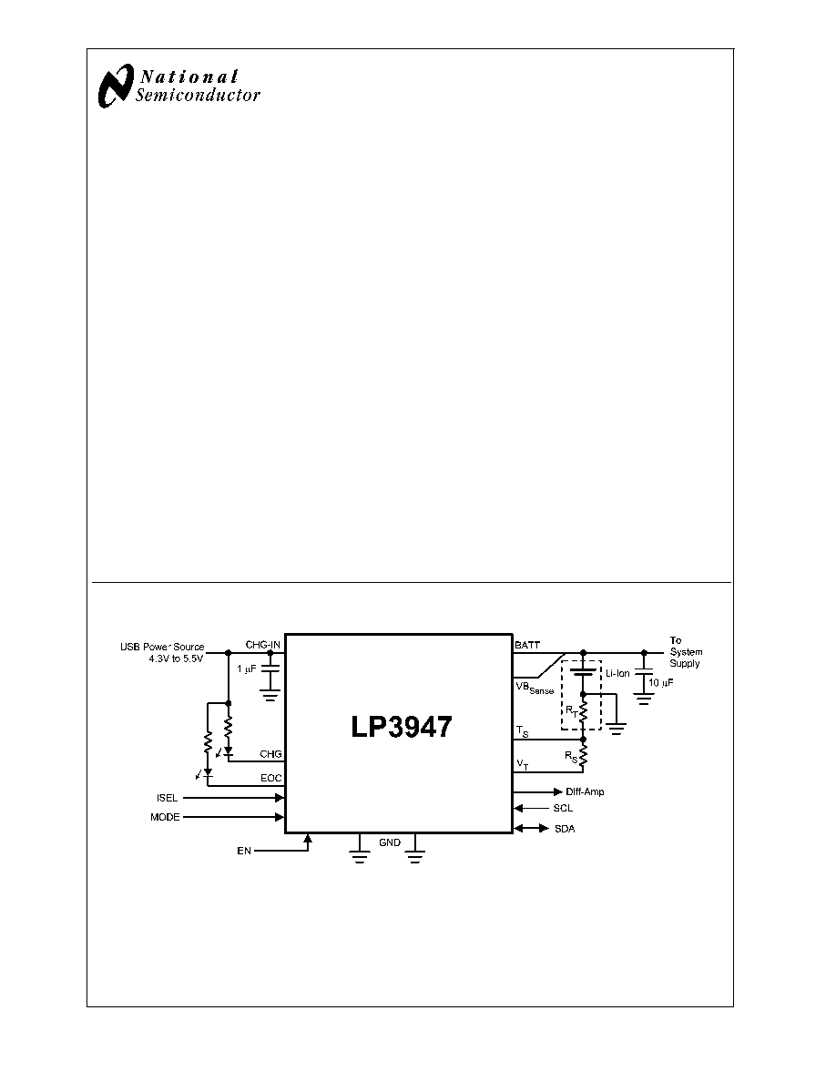
Typical Application Circuit
20111001
More Application Circuit can be found in the Application Note section.
November 2004
LP3947
USB/AC
Adaptor
,
Single
Cell
Li-Ion
Battery
Charger
IC
© 2004 National Semiconductor Corporation
DS201110
www.national.com
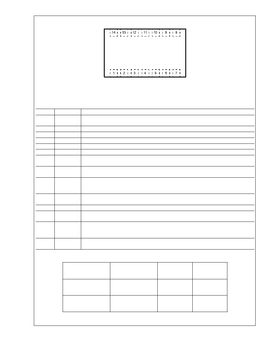
Connection Diagrams and Package Mark Information
20111002
(Top View)
See NS Package Number SDA14B
Pin Description
Pin #
Name
Description
1
EN
Charger Enable Input. Internally pulled high to CHG-IN pin. A HIGH enables the charger and a
LOW disables the charger.
2
SCL
I
2
C serial Interface Clock input.
3
SDA
I
2
C serial Interface Data input/out.
4
BATT
Battery supply input terminal. Must have 10 µF ceramic capacitor to GND
5
V
T
Regulated 2.78V output used for biasing the battery temperature monitoring thermistor.
6
VB
SENSE
Battery Voltage Sense connected to the positive terminal of the battery.
7
MODE
Select pin between AC adaptor and USB port. A LOW sets the LP3947 in USB port and a HIGH
sets it in the AC adaptor.
8
Diff-Amp
Charge current monitoring differential amplifier output. Voltage output representation of the charge
current.
9
Ts
Multi function pin. Battery temperature monitoring input and LDO/Charger mode.
Pulling this pin to V
T
, or removing the thermistor by physically disconnecting the battery, sets the
device in LDO mode.
10
EOC
Active Low Open Drain Output. Active when USB port or AC adaptor is connected and battery is
fully charged. For more information, refer to "LED Charge Status Indicators" section.
11
GND
Ground
12
CHG
Active Low Open Drain Output. Active when USB port or AC adaptor is connected and battery is
being charged. For more information, refer to "LED Charge Status Indicators" section.
13
ISEL
Control pin to switch between low power (100 mA) mode and high power (500 mA) mode in USB
mode. This pin is pulled high internally as default to set the USB in 100 mA mode. This pin has to
be externally pulled low to go into 500 mA mode.
14
CHG-IN
Charger input from a regulated, current limited power source. Must have a 1 µF ceramic capacitor
to GND
Ordering Information
LP3947
Supplied as 1000 Units,
Tape and Reel
LP3947
Supplied as 4500 Units
Tape and Reel
Default
Options*
Package
Marking
LP3947ISD-09
LP3947ISDX-09
I
CHG
= 500 mA
V
BATT
= 4.1V
EOC = 0.1C
L00055B
LP3947ISD-51
LP3947ISDX-51
I
CHG
= 500 mA
V
BATT
= 4.2V
EOC = 0.1C
L00056B
*Other default options are available. Please contact National Semiconductor sales office/distributors for availability and specifications.
LP3947
www.national.com
2
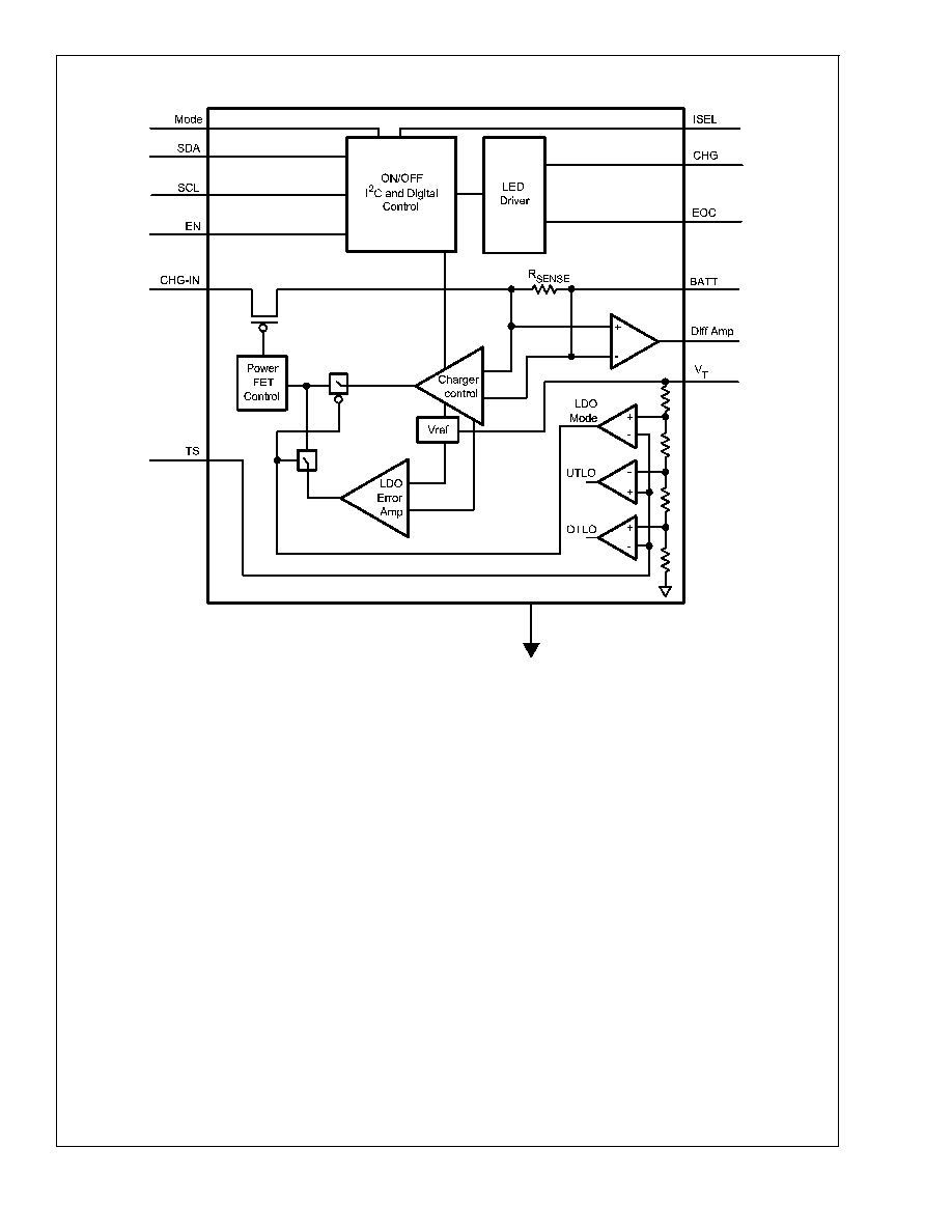
LP3947 Functional Block Diagram
20111003
LP3947
www.national.com
3

Absolute Maximum Ratings
(Notes 1,
2)
If Military/Aerospace specified devices are required,
please contact the National Semiconductor Sales Office/
Distributors for availability and specifications.
CHG-IN
-0.3V to +6.5V
All pins except GND and CHG-IN
(Note 3)
-0.3V to +6V
Junction Temperature
150∞C
Storage Temperature
-40∞C to +150∞C
Power Dissipation (Note 4)
1.89W
ESD (Note 5)
Human Body Model
Machine Model
2 kV
200V
Operating Ratings
(Notes 1, 2)
CHG-IN
0.3V to 6.5V
EN, ISEL, MODE, SCL, SDA,
V
T
(Note 3)
0V to 6V
Junction Temperature
-40∞C to +125∞C
Operating Temperature
-40∞C to +85∞C
Thermal Resistance
JA
37∞C/W
Maximum Power Dissipation
(Note 6)
1.21W
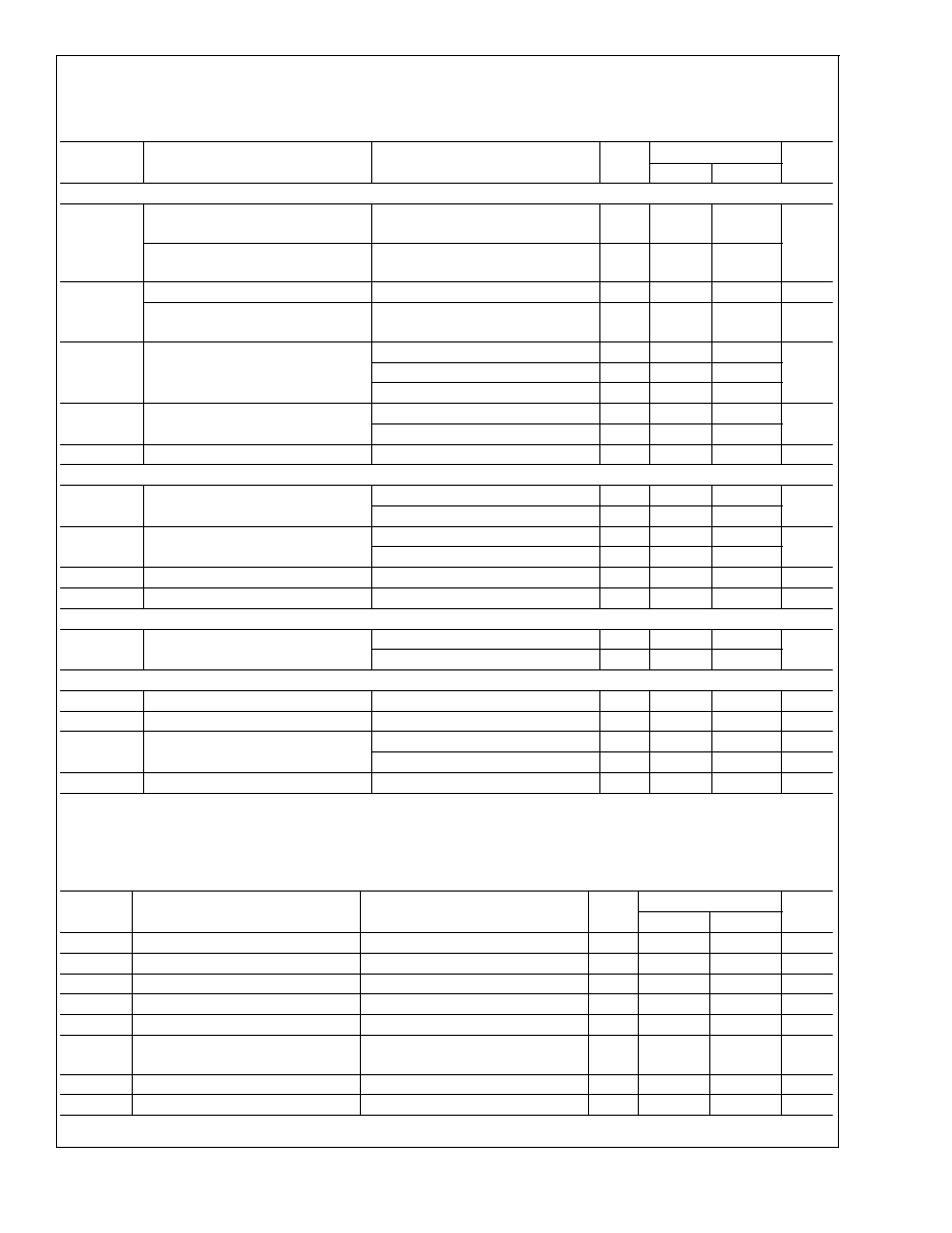
Electrical Characteristics
Unless otherwise noted, V
CHG-IN
= 5V, V
BATT
= 4V, C
CHG-IN
= 1 µF, C
BATT
= 10 µF. Typical values and limits appearing in nor-
mal type apply for T
J
= 25∞C. Limits appearing in boldface type apply over the entire junction temperature range for operation,
T
J
= -40∞C to +85∞C. (Notes 7, 8, 9)
Symbol
Parameter
Conditions
Typ
Limit
Units
Min
Max
V
CC
SUPPLY
V
CHG-IN
Input Voltage Range
4.5
6
V
V
USB
4.3
6
I
CC
Quiescent Current
V
CHG-IN
4V
2
20
µA
EOC = Low, adaptor connected,
V
BATT
= 4.1V
50
150
V
OK-TSHD
Adaptor OK Trip Point (CHG-IN)
V
CHG-IN
≠V
BATT
(Rising)
60
mV
V
CHG-IN
≠V
BATT
(Falling)
50
mV
V
UVLO-TSHD
Under Voltage Lock-Out Trip Point
V
CHG-IN
(Rising)
3.95
3.6
4.3
V
V
CHG-IN
(Falling)
3.75
3.4
4.1
V
V
OVLO-TSHD
Over Voltage Lock-Out Trip Point
V
CHG-IN
(Rising)
5.9
V
V
CHG-IN
(Falling)
5.7
Thermal Shutdown Temperature
(Note 8)
160
∞C
Thermal Shutdown Hysteresis
20
BATTERY CHARGER
I
CHG
Fast Charge Current Range
ISEL = High, In USB Mode
100
mA
ISEL = Low, In USB Mode
500
In AC Adaptor Mode
100
750
Fast Charge Current Accuracy
I
CHARGE
= 100 mA or 150 mA
-20
+20
mA
I
CHARGE
200 mA
-10
+10
%
I
PRE-CHG
Pre-Charge Current
V
BATT
= 2V
45
70
mA
I
EOC
End of Charge Current Accuracy
100 mA to 450 mA, 0.1C EOC Only
(Note 10)
-10
+10
mA
500 mA to 750 mA, All EOC Points
-20
+20
%
V
BATT
Battery Regulation Voltage (For 4.1V
Cell)
T
J
= 0∞C to +85∞C
4.1
4.059
4.141
V
T
J
= -40∞C to +85∞C
4.1
4.038
4.162
Battery Regulation Voltage (For 4.2V
Cell)
T
J
= 0∞C to +85∞C
4.1
4.158
4.242
T
J
= -40∞C to +85∞C
4.2
4.137
4.263
V
CHG-Q
Full Charge Qualification Threshold
V
BATT
Rising, Transition from
Pre-Charge to Full Current
3.0
V
LP3947
www.national.com
4
Electrical Characteristics
(Continued)
Unless otherwise noted, V
CHG-IN
= 5V, V
BATT
= 4V, C
CHG-IN
= 1 µF, C
BATT
= 10 µF. Typical values and limits appearing in nor-
mal type apply for T
J
= 25∞C. Limits appearing in boldface type apply over the entire junction temperature range for operation,
T
J
= -40∞C to +85∞C. (Notes 7, 8, 9)
Symbol
Parameter
Conditions
Typ
Limit
Units
Min
Max
BATTERY CHARGER
V
BAT-RST
Restart Threshold Voltage
(For 4.1V Cell)
V
BATT
Falling, Transition from EOC,
to Pre-Qualification State
3.9
3.77
4.02
V
Restart Threshold Voltage
(For 4.2V Cell)
V
BATT
Falling, Transition from EOC,
to Pre-Qualification State
4.00
3.86
4.12
R
SENSE
Internal Current Sense Resistance
(Note 8)
120
m
Internal Current Sense Resistor
Load Current
1.2
A
ICHG
MON
Diff-Amp Output
I
CHG
= 50 mA
0.583
V
I
CHG
= 100 mA
0.663
I
CHG
= 750 mA
1.790
t
OUT
Charger Time Out
T
J
= 0∞C to 85∞C
5.625
4.78
6.42
Hrs
T
J
= -40∞C to +85∞C
5.625
4.5
6.75
V
OL
Low Level Output Voltage
EOC, CHG Pins each at 9 mA
100
mV
TEMPERATURE SENSE COMPARATORS
V
UTLO
Low Voltage Threshold
Voltage at Ts Pin, Rising
2.427
V
Voltage at Ts Pin, Falling
2.369
V
OTLO
High Voltage Threshold
Voltage at Ts Pin, Rising
1.470
V
Voltage at Ts Pin, Falling
1.390
V
LDO
LDO Mode Voltage Threshold
Voltage at Ts Pin, % of V
T
97
%
V
T
Voltage Output
2.787
V
LDO MODE (Ts = HIGH)
V
OUT
Output Voltage Regulation
I
LOAD
= 50 mA
4.10
V
I
LOAD
= 750 mA
4.06
LOGIC LEVELS
V
IL
Low Level Input Voltage
EN, ISEL, MODE
0.4
V
V
IH
High Level Input Voltage
EN, ISEL, MODE
2.0
V
I
IL
Input Current
EN, ISEL = LOW
-10
+10
µA
MODE = LOW
-5
+5
µA
I
IH
Input Current
EN, ISEL, MODE = HIGH
-5
+5
µA
Electrical Characteristics, I
2
C Interface
Unless otherwise noted, V
CHG-IN
= V
DD
= 5V, V
BATT
= 4V. Typical values and limits appearing in normal type apply for T
J
=
25∞C. Limits appearing in boldface type apply over the entire junction temperature range for operation, T
J
= -40∞C to +125∞C.
(Notes 7, 8, 9)
Symbol
Parameter
Conditions
Typ
Limit
Units
Min
Max
V
IL
Low Level Input Voltage
SDA & SCL (Note 8)
0.4
0.3 V
DD
V
V
IH
High Level Input Voltage
SDA & SCL (Note 8)
0.7 V
DD
V
DD
+0.5
V
V
OL
Low Level Output Voltage
SDA & SCL (Note 8)
0
0.2 V
DD
V
V
HYS
Schmitt Trigger Input Hysteresis
SDA & SCL (Note 8)
0.1 V
DD
V
F
CLK
Clock Frequency
(Note 8)
400
kHz
t
HOLD
Hold Time Repeated START
Condition
(Note 8)
0.6
µs
t
CLK-LP
CLK Low Period
(Note 8)
1.3
µs
t
CLK-HP
CLK High Period
(Note 8)
0.6
µs
LP3947
www.national.com
5