LP3954
Advanced Lighting Management Unit
General Description
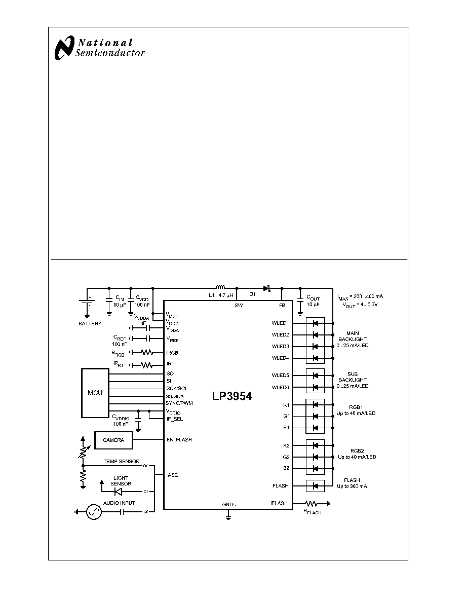
LP3954 is an advanced lighting management unit for hand-
held devices. It drives any phone lights including display
backlights, RGB, keypad and camera flash LEDs. The boost
DC-DC converter drives high current loads with high effi-
ciency. White LED backlight drivers are high efficiency low
voltage structures with excellent matching and automatic
fade in/ fade out function. The new stand-alone command
based RGB controller is feature rich and easy to configure.
Built-in audio synchronization feature allows user to synchro-
nize the color LEDs to audio input. Integrated high current
driver can drive camera flash LED or motor/vibra. Internal
ADC can be used for ambient light or temperature sensing.
The flexible SPI/I
2
C interface allows easy control of LP3954.
Small micro SMD package together with minimum number of
external components is a best fit for handheld devices.
Features
n
Audio synchronization for color/RGB LEDs
n
Command based PWM controlled RGB LED drivers
n
High current driver for flash LED with built-in timing.
n
4+2 or 6 low voltage constant current white LED drivers
with programmable 8-bit adjustment (0...25mA/LED)
n
High efficiency Boost DC-DC converter
n
SPI / I
2
C compatible interface
n
Possibility for external PWM dimming control
n
Possibility for clock synchronization for RGB timing
n
Ambient light and temperature sensing possibility
n
Small package ≠ 36 bump micro SMD,
3.0mm*3.0mm*0.6mm
Applications
n
Cellular Phones
n
PDAs, MP3 players
Typical Applications
20132260
June 2005
LP3954
Advanced
Lighting
Management
Unit
© 2005 National Semiconductor Corporation
DS201322
www.national.com
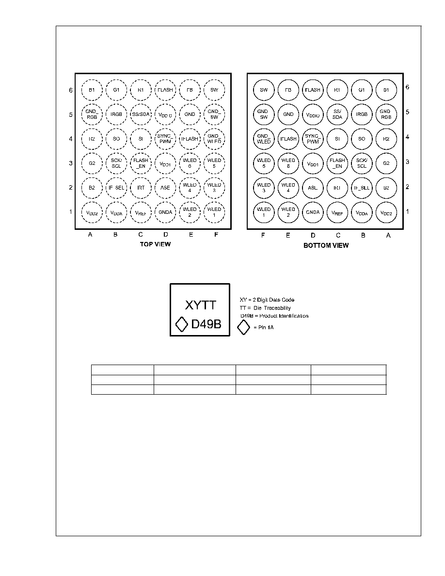
Connection Diagrams and Package Mark Information
(Continued)
PIN DESCRIPTION
Pin #
Name
Type
Description
6F
SW
Output
Boost Converter Power Switch
6E
FB
Input
Boost Converter Feedback
6D
FLASH
Output
High Current Flash Output
6C
R1
Output
Red LED 1 Output
6B
G1
Output
Green LED 1 Output
6A
B1
Output
Blue LED 1 Output
5F
GND_SW
Ground
Power Switch Ground
5E
GND
Ground
Ground
5D
VDDIO
Power
Supply Voltage for Input/output Buffers and Drivers
5C
SS/SDA
Logic Input/Output
Slave Select (SPI), Serial Data In/Out (I
2
C)
5B
IRGB
Input
Bias Current Set Resistor for RGB Drivers
5A
GND_RGB
Ground
Ground for RGB Currents
4F
GND_WLED
Ground
Ground for WLED Currents
4E
IFLASH
Input
High Current Flash Current Set Resistor
4D
SYNC_PWM
Logic Input
External PWM Control for LEDs or External Clock for RGB Sync
4C
SI
Logic Input
Serial Input (SPI), Address Select (I
2
C)
4B
SO
Logic Output
Serial Data Out (SPI)
4A
R2
Output
Red LED 2 output
3F
WLED5
Output
White LED 5 output
3E
WLED6
Output
White LED 6 output
3D
VDD1
Power
Supply voltage
3C
EN_FLASH
Logic Input
Enable for High Current Flash
3B
SCK/SCL
Logic Input
Clock (SPI/I
2
C)
3A
G2
Output
Green LED 2 Output
2F
WLED3
Output
White LED 3 output
2E
WLED4
Output
White LED 4 output
2D
ASE
Input
Audio Synchronization Input
2C
IRT
Input
Oscillator Frequency Resistor
2B
IF_SEL
Logic Input
Interface (SPI or I
2
C compatible) Selection (IF_SEL = 1 for SPI)
2A
B2
Output
Blue LED 2 Output
1F
WLED1
Output
White LED 1 Output
1E
WLED2
Output
White LED 2 Output
1D
GNDA
Ground
Ground for Analog Circuitry
1C
VREF
Output
Reference Voltage
1B
VDDA
Power
Internal LDO Output
1A
VDD2
Power
Supply Voltage
LP3954
www.national.com
3

Absolute Maximum Ratings
(Notes 1,
2)
If Military/Aerospace specified devices are required,
please contact the National Semiconductor Sales Office/
Distributors for availability and specifications.
V (SW, FB, R1-2, G1-2, B1-2,
FLASH, WLED1-6)(Notes 3, 4)
-0.3V to +7.2V
V
DD1
, V
DD2
, V
DD_IO
, V
DDA
-0.3V to +6.0V
Voltage on ASE, IRT, IFLASH,
IRGB, VREF
-0.3V to V
DD1
+0.3V
with 6.0V max
Voltage on Logic Pins
-0.3V to V
DD_IO
+0.3V with 6.0V max
V(all other pins): Voltage to GND
-0.3V to 6.0V
I (V
REF
)
10µA
I(R1, G1, B1, R2, G2, B2)
100mA
I(FLASH)(Note 5)
400mA
Continuous Power
Dissipation(Note 6)
Internally Limited
Junction Temperature (T
J-MAX
)
150
o
C
Storage Temperature Range
-65
o
C to +150
o
C
Maximum Lead Temperature
(Soldering) (Note 7)
260
o
C
ESD Rating (Note 8)
Human Body Model:
2kV
Operating Ratings
(Notes 1, 2)
V (SW, FB, WLED1-6, R1-2,
G1-2, B1-2, FLASH)
0 to 6.0V
V
DD1,2
with external LDO
2.7 to 5.5V
V
DD1,2
with internal LDO
3.0 to 5.5V
V
DDA
2.7 to 2.9V
V
DD_IO
1.65V to V
DD1
Voltage on ASE
0.1V to V
DDA
≠0.1V
Recommended Load Current
0mA to 300mA
Junction Temperature (T
J
) Range
-30
o
C to +125
o
C
Ambient Temperature (T
A
)
Range(Note 9)
-30
o
C to +85
o
C
Thermal Properties
Junction-to-Ambient Thermal
Resistance(
JA
), TLA36AAA
Package
(Note 10)
60
o
C/W
LP3954
www.national.com
4

Electrical Characteristics
(Notes 2, 11)
Limits in standard typeface are for T
J
= 25
o
C. Limits in boldface type apply over the operating ambient temperature range
(-30
o
C
<
T
A
<
+85
o
C). Unless otherwise noted, specifications apply to the LP3954 Block Diagram with: V
DD1
= V
DD2
=
3.6V, V
DDIO
= 2.8V, C
VDD
= C
VDDIO
= 100nF, C
OUT
= C
IN
= 10µF, C
VDDA
= 1µF, C
REF
= 100nF, L
1
= 4.7µH, R
FLASH
=1.2k,
R
RGB
=5.6k and R
RT
=82k (Note 12).
Symbol
Parameter
Condition
Min
Typ
Max Units
I
VDD
Standby supply current
(V
DD1
, V
DD2
)
NSTBY = L
SCK, SS, SI
1
8
µA
No-boost supply current
(V
DD1
, V
DD2
)
NSTBY = H,
EN_BOOST = L
SCK, SS, SI
Audio sync and LEDs OFF
400
µA
No-load supply current
(V
DD1
, V
DD2
)
NSTBY = H,
EN_BOOST = H
SCK, SS, SI
Audio sync and LEDs OFF
Autoload OFF
1
mA
RGB drivers
(V
DD1
, V
DD2
)
CC mode at R1, G1, B1 and R2, G2, B2 set to 15mA
150
µA
SW mode
150
WLED drivers
(V
DD1
, V
DD2
)
4+2 banks I
OUT
/LED 25mA
500
µA
Audio synchronization
(V
DD1
, V
DD2
)
Audio sync ON
µA
V
DD1,2
= 2.8V
390
V
DD1,2
= 3.6V
700
Flash
(V
DD1
, V
DD2
)
I(R
FLASH
)=1mA
Peak current during flash
2
mA
I
VDDIO
V
DDIO
Standby Supply
current
NSTBY = L
SCK, SS, SI = H
1
µA
V
DDIO
supply current
1MHz SCK frequency in SPI mode, C
L
= 50pF at SO pin
20
µA
I
EXT_LDO
External LDO output current
(V
DD1
, V
DD2
, V
DDA
)
7V tolerant application only
I
BOOST
= 300mA
6.5
mA
V
DDA
Output voltage of internal
LDO for analog parts
(Note 13)
2.72 2.80 2.88
V
-3
+3
%
Note 1: Absolute Maximum Ratings indicate limits beyond which damage to the component may occur. Operating Ratings are conditions under which operation of
the device is guaranteed. Operating Ratings do not imply guaranteed performance limits. For guaranteed performance limits and associated test conditions, see the
Electrical Characteristics tables.
Note 2: All voltages are with respect to the potential at the GND pins.
Note 3: Battery/Charger voltage should be above 6V no more than 10% of the operational lifetime.
Note 4: Voltage tolerance of LP3954 above 6.0V relies on fact that V
DD1
and V
DD2
(2.8V) are available (ON) at all conditions. If V
DD1
and V
DD2
are not available
(ON) at all conditions, National Semiconductor does not guarantee any parameters or reliability for this device.
Note 5: The total load current of the boost converter in worst-case conditions should be limited to 300mA (min. input and max. output voltage).
Note 6: Internal thermal shutdown circuitry protects the device from permanent damage. Thermal shutdown engages at T
J
=160
o
C (typ.) and disengages at
T
J
=140
o
C (typ.).
Note 7: For detailed soldering specifications and information, please refer to National Semiconductor Application Note AN1112 : Micro SMD Wafer Level Chip Scale
Package
Note 8: The Human body model is a 100pF capacitor discharged through a 1.5k
resistor into each pin. The machine model is a 200pF capacitor discharged
directly into each pin. MIL-STD-883 3015.7
Note 9: In applications where high power dissipation and/or poor package thermal resistance is present, the maximum ambient temperature may have to be
derated. Maximum ambient temperature (T
A-MAX
) is dependent on the maximum operating junction temperature (T
J-MAX-OP
= 125
o
C), the maximum power
dissipation of the device in the application (P
D-MAX
), and the junction-to ambient thermal resistance of the part/package in the application (
JA
), as given by the
following equation: T
A-MAX
= T
J-MAX-OP
≠ (
JA
x P
D-MAX
).
Note 10: Junction-to-ambient thermal resistance is highly application and board-layout dependent. In applications where high maximum power dissipation exists,
special care must be paid to thermal dissipation issues in board design.
Note 11: Min and Max limits are guaranteed by design, test, or statistical analysis. Typical numbers are not guaranteed, but do represent the most likely norm.
Note 12: Low-ESR Surface-Mount Ceramic Capacitors (MLCCs) used in setting electrical characteristics.
Note 13: V
DDA
output is not recommended for external use.
LP3954
www.national.com
5