LP3958
Lighting Management Unit with High Voltage Boost
Converter
General Description
LP3958 is a Lighting Management Unit for portable applica-
tions. It is used to drive display backlight and keypad LEDs.
The device can drive 5 separately connected strings of LEDs
with high voltage boost converter.
The keypad LED driver allows driving LEDs from high volt-
age boost converter or separate supply voltage.The MAIN
and SUB outputs are high resolution current mode drivers.
Keypad LED outputs can be used in switch mode and cur-
rent mode. External PWM control can be used for any se-
lected outputs.
The device is controlled through 2-wire low voltage I
2
C
compatible interface that reduces the number of required
connections.
LP3958 is offered in a tiny 25-bump micro-SMD package.
Features
n
High efficiency boost converter with programmable
output voltage
n
2 individual drivers for serial display backlight LEDs
n
3 drivers for serial keypad LEDs
n
Automatic dimming controller
n
Stand alone serial keypad LEDs controller
n
3 general purpose IO pins
n
25-bump micro SMD Package: (2.54mm x 2.54mm x
0.6mm)
Applications
n
Cellular Phones and PDAs
n
MP3 Players
n
Digital Cameras
Typical Application
20175570
February 2006
LP3958
Lighting
Management
Unit
with
High
V
oltage
Boost
Converter
© 2006 National Semiconductor Corporation
DS201755
www.national.com
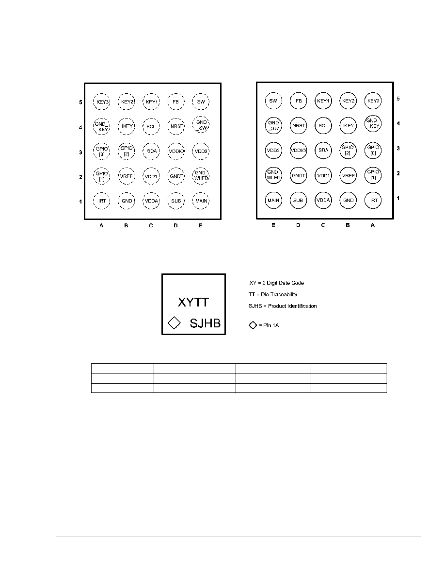
Connection Diagrams and Package Mark Information
(Continued)
PIN DESCRIPTIONS
Pin #
Name
Type
Description
5E
SW
Output
Boost Converter Power Switch
5D
FB
Input
Boost Converter Feedback
5C
KEY1
Output
Keypad LED Output 1 (Current Sink)
5B
KEY2
Output
Keypad LED Output 2 (Current Sink)
5A
KEY3
Output
Keypad LED Output 3 (Current Sink)
4E
GND_SW
Ground
Power Switch Ground
4D
NRST
Input
External Reset, Active Low
4C
SCL
Logic Input
Clock Input for I
2
C Compatible Interface
4B
IKEY
Input
External Keypad LED Maximum Current Set Resistor
4A
GND_KEY
Ground
Ground for KEY LED Currents
3E
VDD2
Power
Supply Voltage 3.0...5.5 V
3D
VDDIO
Power
Supply Voltage for Digital Input/Output Buffers and Drivers
3C
SDA
Logic Input/Output
Data Input/Output for I
2
C Compatible Interface
3B
GPIO[2]
Logic Input/Output
General Purpose Logic Input/Output
3A
GPIO[0] / PWM
Logic Input/Output
General Purpose Logic Input/Output / External PWM Input
2E
GND_WLED
Ground
Ground for White LED Currents (MAIN and SUB Outputs)
2D
GNDT
Ground
Ground
2C
VDD1
Power
Supply Voltage 3.0...5.5 V
2B
VREF
Output
Reference Voltage (1.23V)
2A
GPIO[1]
Logic Input/Output
General Purpose Logic Input/Output
1E
MAIN
Output
MAIN Display White LED Current Output (Current Sink)
1D
SUB
Output
SUB Display White LED Current Output (Current Sink)
1C
VDDA
Output
Internal LDO Output (2.80V)
1B
GND
Ground
Ground for Core Circuitry
1A
IRT
Input
Oscillator Frequency Set Resistor
LP3958
www.national.com
3

Absolute Maximum Ratings
(Notes 1,
2)
If Military/Aerospace specified devices are required,
please contact the National Semiconductor Sales Office/
Distributors for availability and specifications.
V (SW, FB, MAIN, SUB, KEY1,
KEY2, KEY3)
-0.3V to +20V
V
DD1
, V
DD2
, V
DDIO
, V
DDA
-0.3V to +6.0V
Voltage on I
KEY
, I
RT
, V
REF
-0.3V to V
DD1
+0.3V
with 6.0V max
Voltage on Logic Pins
-0.3V to V
DDIO
+0.3V
with 6.0V max
I (V
REF
)
10µA
I(KEY1, KEY2, KEY3)
100mA
Continuous Power Dissipation
(Note 3)
Internally Limited
Junction Temperature (T
J-MAX
)
125
o
C
Storage Temperature Range
-65
o
C to +150
o
C
Maximum Lead Temperature
(Soldering) (Note 4)
260
o
C
ESD Rating (Note 5)
Human Body Model:
2kV
Machine Model:
200V
Operating Ratings
(Notes 1, 2)
V (SW, FB, MAIN, SUB)
0 to +19V
V
DD1,2
3.0 to 5.5V
V
DDIO
1.65V to V
DD1
Recommended Load Current
(KEY1, KEY2, KEY3) CC Mode
0mA to 15mA/driver
Recommended Total Boost
Converter Load Current
0mA to 70mA
Junction Temperature (T
J
) Range
-30
o
C to +125
o
C
Ambient Temperature (T
A
) Range
(Note 6)
-30
o
C to +85
o
C
Thermal Properties
Junction-to-Ambient Thermal
Resistance(
JA
), TLA25 Package
(Note 7)
60 - 100
o
C/W
LP3958
www.national.com
4
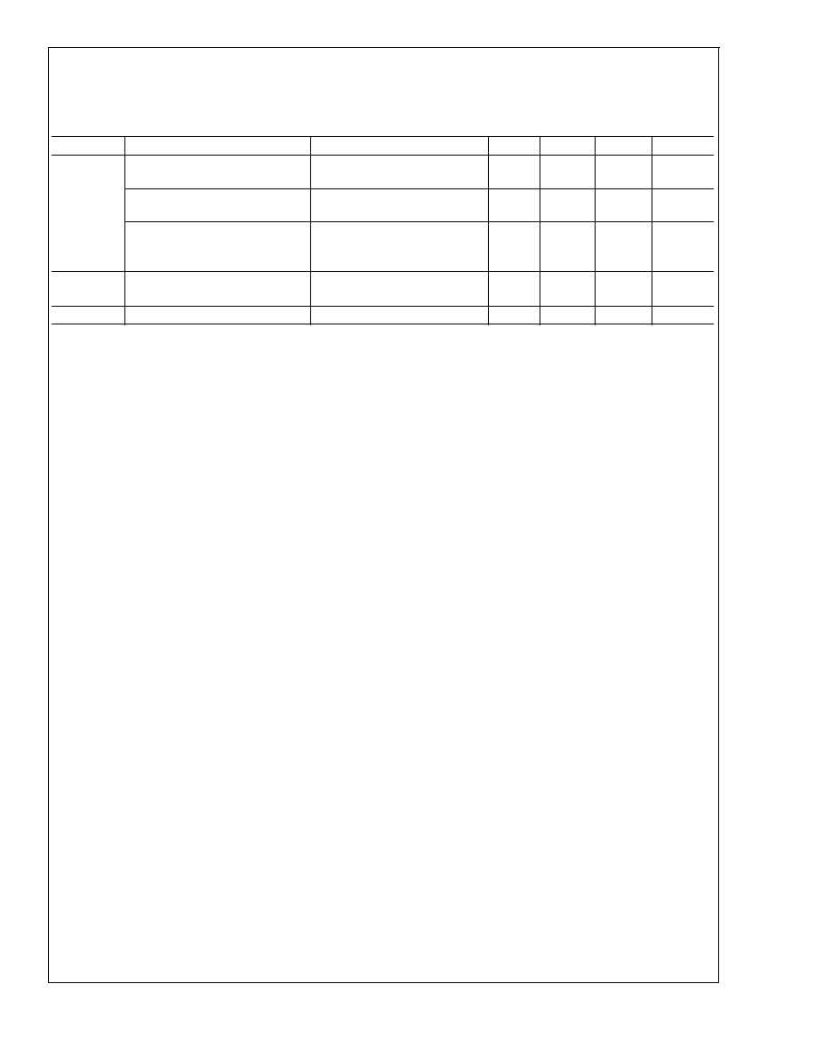
Electrical Characteristics
(Notes 2, 8)
Limits in standard typeface are for T
J
= 25
o
C. Limits in boldface type apply over the operating ambient temperature range
(-30
o
C
<
T
A
<
+85
o
C). Unless otherwise noted, specifications apply to the LP3958 Block Diagram with: V
DD1,2
= 3.0 ... 5.5V,
C
VDD
= C
VDDIO
= 100nF, C
OUT
= 2 x 4.7µF, C
IN
= 10µF, C
VDDA
= 1µF, C
VREF
= 100nF, L1 = 10µH, R
KEY
= 8.2k
and R
RT
=
82k
(Note 9).
Symbol
Parameter
Condition
Min
Typ
Max
Units
I
VDD
Standby supply current
(V
DD1
, V
DD2
)
NSTBY = L
Register 0DH=08H (Note 10)
1.7
7
µA
No-boost supply current
(V
DD1
, V
DD2
)
NSTBY = H,
EN_BOOST = L
300
800
µA
No-load supply current
(V
DD1
, V
DD2
)
NSTBY = H,
EN_BOOST = H
Autoload OFF
750
1300
uA
V
DDA
Output voltage of internal LDO
I
VDDA
= 1mA
2.80
V
-3
+3
%
V
REF
Reference voltage (Note 11)
1.23
V
Note 1: Absolute Maximum Ratings indicate limits beyond which damage to the component may occur. Operating Ratings are conditions under which operation of
the device is guaranteed. Operating Ratings do not imply guaranteed performance limits. For guaranteed performance limits and associated test conditions, see the
Electrical Characteristics tables.
Note 2: All voltages are with respect to the potential at the GND pins.
Note 3: Internal thermal shutdown circuitry protects the device from permanent damage. Thermal shutdown engages at T
J
=150
o
C (typ.) and disengages at
T
J
=130
o
C (typ.).
Note 4: For detailed soldering specifications and information, please refer to National Semiconductor Application Note AN1112 : Micro SMD Wafer Level Chip Scale
Package
Note 5: The Human body model is a 100pF capacitor discharged through a 1.5k
resistor into each pin. The machine model is a 200pF capacitor discharged
directly into each pin. MIL-STD-883 3015.7
Note 6: In applications where high power dissipation and/or poor package thermal resistance is present, the maximum ambient temperature may have to be
derated. Maximum ambient temperature (T
A-MAX
) is dependent on the maximum operating junction temperature (T
J-MAX-OP
= 125
o
C), the maximum power
dissipation of the device in the application (P
D-MAX
), and the junction-to ambient thermal resistance of the part/package in the application (
JA
), as given by the
following equation: T
A-MAX
= T
J-MAX-OP
≠ (
JA
x P
D-MAX
).
Note 7: Junction-to-ambient thermal resistance is highly application and board-layout dependent. In applications where high maximum power dissipation exists,
special care must be paid to thermal dissipation issues in board design.
Note 8: Min and Max limits are guaranteed by design, test, or statistical analysis. Typical numbers are not guaranteed, but do represent the most likely norm.
Note 9: Low-ESR Surface-Mount Ceramic Capacitors (MLCCs) used in setting electrical characteristics.
Note 10: Boost output voltage set to 8V (08H in register 0DH) to prevent any unneccessary current consumption.
Note 11: No external loading allowed for V
REF
pin.
LP3958
www.national.com
5