LP3971
Power Management Unit for Advanced Application
Processors
General Description
The LP3971 is a multi-function, programmable Power Man-
agement Unit, designed especially for advanced application
processors. The LP3971 is optimized for low power hand-
held applications and provides 6 low dropout, low noise
linear regulators, three DC/DC magnetic buck regulators, a
back-up battery charger and two GPIO's. A high speed serial
interface is included to program individual regulator output
voltages as well as on/off control.
Key Specifications
Buck Regulators
n
Programmable V
OUT
from 0.8 to 3.3V
n
Up to 95% efficiency
n
Up to 1.6A output current
n
±
3% output voltage accuracy
LDO's
n
Programmable V
OUT
of 1.0V≠3.3V
n
±
3% output voltage accuracy
n
150/300/370 mA output currents
-- LDO RTC 30 mA
-- LDO 1 300 mA
-- LDO 2 150 mA
-- LDO 3 150 mA
-- LDO 4 150 mA
-- LDO 5 370 mA
n
100 mV (typ) dropout
Features
n
Compatible with advanced applications processors
requiring DVM (Dynamic Voltage Management)
n
Three buck regulators for powering high current
processor functions or I/O's
n
6 LDO's for powering RTC, peripherals, and I/O's
n
Backup battery charger with automatic switch for
lithium-manganese coin cell batteries and Super
capacitors
n
I
2
C compatible high speed serial interface
n
Software control of regulator functions and settings
n
Precision internal reference
n
Thermal overload protection
n
Current overload protection
n
Tiny 40-pin 5x5 mm LLP package
Applications
n
PDA phones
n
Smart phones
n
Personal Media Players
n
Digital cameras
n
Application processors
-- Intel Xscale
-- Freescale
-- Samsung
January 2006
LP3971
Power
Management
Unit
for
Advanced
Application
Processors
© 2006 National Semiconductor Corporation
DS201807
www.national.com
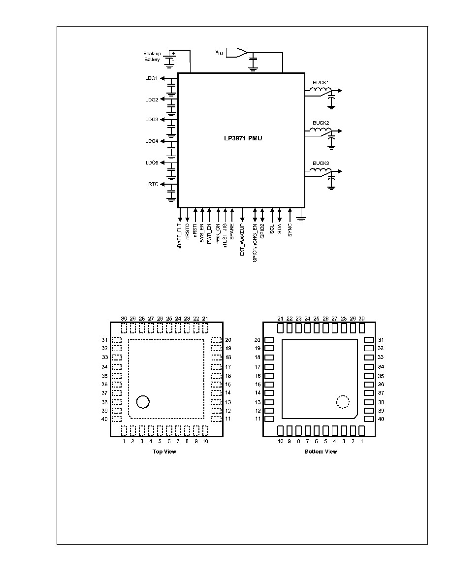
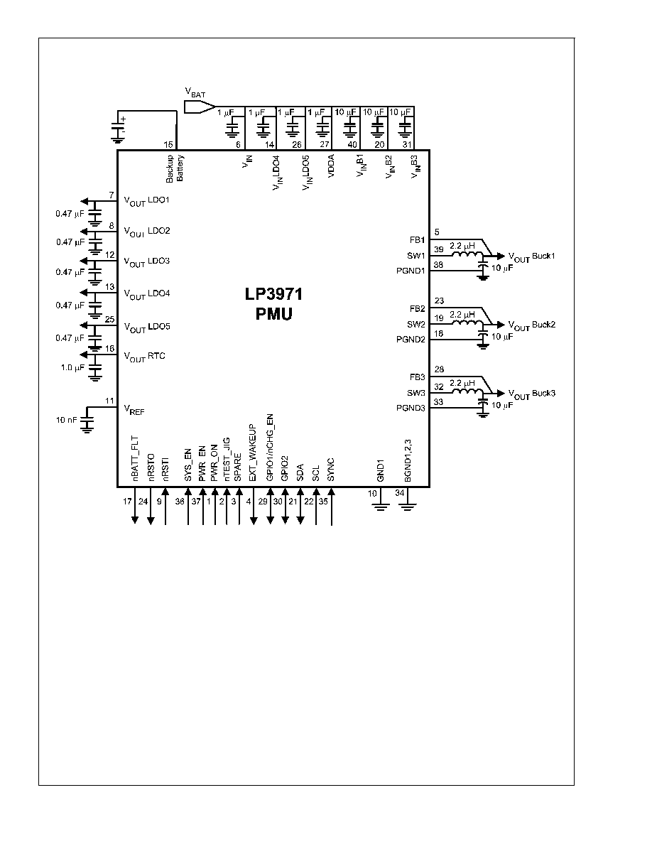
Simplified Application Circuit
20180701
Connection Diagrams and Package Mark Information
40-Pin Leadless Leadframe Package
NS Package Number SQF40A
20180702
Note: Circle marks pin 1 position.
LP3971
www.national.com
2
Connection Diagrams and Package Mark Information
(Continued)
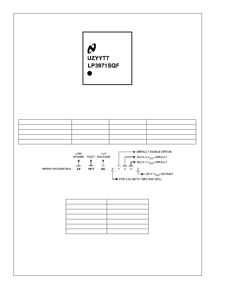
Package Mark
20180704
Top View
Note: The actual physical placement of the package marking will vary from part to part. The package marking "UZYY" designates
the date code. "TT" is a NSC internal code for die traceability. Both will vary considerably. "LP3971SQF" identifies the device (part
number, option, etc.).
Ordering Information
Option
Order Number
Package Marking
Supplied As
Default Voltage version ≠ A**
LP3971SQ-A514
71-A514
250 units, Tape-and-Reel
Default Voltage version ≠ A**
LP3971SQX-A514
71-A514
2500 units, Tape-and-Reel
`Default Voltage version - B
LP3971SQ-B410
71-B410
250 units, Tape-and-Reel
Default Voltage version - B
LP3971SQX-B410
71-B410
2500 units, Tape-and-Reel
** To be Released
20180705
Default V
OUT
Coding
Z
Default V
OUT
0
1.3
1
1.8
2
2.5
3
2.8
4
3.0
5
3.3
LP3971
www.national.com
3
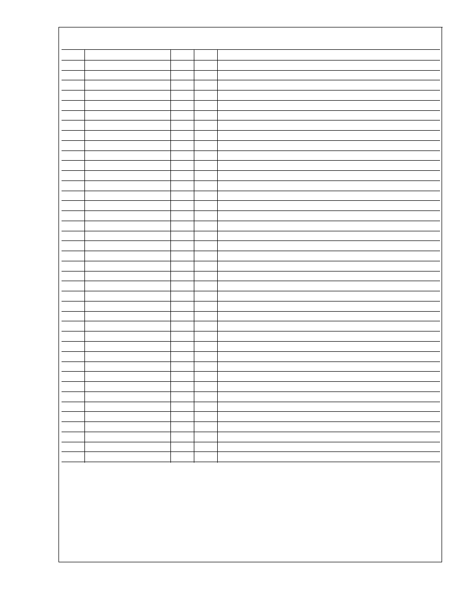
Pin Descriptions
Pin #
Name
I/O
Type
Description
1
PWR_ON
I
D
CPU Wakeup input
2
nTEST_JIG
I
D
CPU Wakeup input
3
SPARE
I
D
CPU Wakeup input
4
EXT_WAKEUP
O
D
CPU Wakeup output
5
FB1
I
A
Buck1 Feedback
6
V
IN
I
P
Battery Input (Internal circuitry and LDO1≠3 power input)
7
V
OUT
LDO1
O
P
LDO1 output
8
V
OUT
LDO2
O
P
LDO2 output
9
nRSTI
I
D
Reset Input
10
GND1
G
G
Ground
11
V
REF
O
A
Bypass Cap. for reference
12
V
OUT
LDO3
O
P
LDO3 output
13
V
OUT
LDO4
O
P
LDO4 output
14
V
IN
LDO4
I
P
Input power for LDO4
15
V
IN
BUBATT
I
P
Back Up Battery input
16
V
OUT
LDO_RTC
O
P
LDO_RTC output
17
nBATT_FLT
O
D
Main Battery fault output
18
PGND2
G
G
Buck2 NMOS Power Ground
19
SW2
O
P
Buck2 Output
20
V
IN
Buck2
I
P
Buck2 battery input
21
SDA
I/O
D
I
2
C Data
22
SCL
I
D
I
2
C Clock
23
FB2
I
A
Buck2 Feedback
24
nRSTO
O
D
Reset output
25
V
OUT
LDO5
O
P
LDO5 output
26
V
IN
LDO5
I
P
Input power for LDO5
27
VDDA
I
P
Analog Power
28
FB3
I
A
Buck3 Feedback
29
GPIO1/nCHG_EN
I/O
D
General Purpose I/O/Ext. backup battery charger enable
30
GPIO2
I/O
D
General Purpose I/O
31
V
IN
Buck3
I
P
Buck3 battery input
32
SW3
O
P
Buck3 Output
33
PGND3
G
G
Buck3 NMOS Power Ground
34
BGND1,2,3
G
G
Bucks 1, 2 and 3 analog Ground
35
SYNC
I
D
Bucks external clock input
36
SYS_EN
I
D
High voltage domain enable
37
PWR_EN
I
D
Low Voltage domain enable
38
PGND1
G
G
Buck1 NMOS Power Ground
39
SW1
O
P
Buck1 Output
40
V
IN
Buck1
I
P
Buck1 battery input
A: Analog Pin
D: Digital Pin
G: Ground Pin
P: Power Pin
I: Input Pin
I/O: Input/Output Pin
O: Output Pin
Note: In this document active low logic items are prefixed with a lowercase "n"
LP3971
www.national.com
4
Applications Schematic Diagrams
Diagram 1 LDO 4 and LDO5 Connected To V
BATTERY
20180706
See Application Hints for recommended external components and component selection
** NOTE: RTC LDO ≠ In applications when Vbatt drops below 1.7V (ie. removing the main battery), system reset will be enabled. To void this situation, replace the
RTC LDO (pin 16) 1.0uF capacitor with a 10uF capacitor.
LP3971
www.national.com
5