LP3982
Micropower, Ultra Low-Dropout, Low-Noise, 300mA
CMOS Regulator
General Description
The LP3982 low-dropout (LDO) CMOS linear regulator is
available in 1.8V, 2.5V, 2.77V, 2.82V, 3.0V, 3.3V, and adjust-
able versions. They deliver 300mA of output current. Pack-
aged in an 8-Pin MSOP, the LP3982 is pin and package
compatible with Maxim's MAX8860. The LM3982 is also
available in the small footprint LLP package.
The LP3982 suits battery powered applications because of
its shutdown mode (1nA typ), low quiescent current (90µA
typ), and LDO voltage (120mV typ). The low dropout voltage
allows for more utilization of a battery's available energy by
operating closer to its end-of-life voltage. The LP3982's
PMOS output transistor consumes relatively no drive current
compared to PNP LDO regulators.
This PMOS regulator is stable with small ceramic capacitive
loads (2.2µF typ).
These devices also include regulation fault detection, a
bandgap voltage reference, constant current limiting and
thermal overload protection.
Features
n
MAX8860 pin, package and spec. compatible
n
LLP space saving package
n
300mA guaranteed output current
n
120mV typical dropout
@
300mA
n
90µA typical quiescent current
n
1nA typical shutdown mode
n
60dB typical PSRR
n
2.5V to 6V input range
n
120µs typical turn-on time
n
Stable with small ceramic output capacitors
n
37µV RMS output voltage noise (10Hz to 100kHz)
n
Over temperature/over current protection
n
±
2% output voltage tolerance
Applications
n
Wireless handsets
n
DSP core power
n
Battery powered electronics
n
Portable information appliances
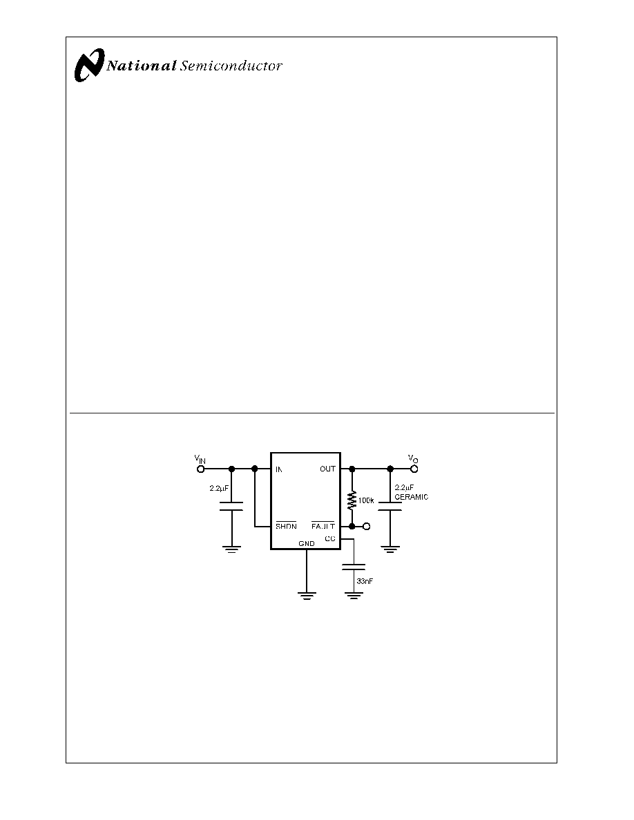
Application Circuit
20036931
July 2002
LP3982
Micropower
,
Ultra
Low-Dropout,
Low-Noise,
300mA
CMOS
Regulator
© 2002 National Semiconductor Corporation
DS200369
www.national.com
Absolute Maximum Ratings
(Notes 1,
2)
If Military/Aerospace specified devices are required,
please contact the National Semiconductor Sales Office/
Distributors for availability and specifications.
V
IN
, V
OUT
, V
SHDN
, V
SET
, V
CC
,
V
FAULT
-0.3V to 6.5V
Fault Sink Current
20mA
Power Dissipation
(Note 3)
Storage Temperature Range
-65∞C to 160∞C
Junction Temperature (T
J
)
150∞C
Lead Temperature (10 sec.)
260∞C
ESD Rating
Human Body Model (Note 6)
2kV
Machine Model
200V
Thermal Resistance (
JA
)
8-Pin MSOP
223∞C/W
8-Pin LLP
(Note 3)
Operating Ratings
(Note 1)
,
(Note 2)
Temperature Range
-40∞C to 85∞C
Supply Voltage
2.5V to 6.0V
Electrical Characteristics
Unless otherwise specified, all limits guaranteed for V
IN
= V
O
+0.5V (Note 7), V
SHDN
= V
IN
, C
IN
= C
OUT
= 2.2µF, C
CC
= 33nF,
T
J
= 25∞C. Boldface limits apply for the operating temperature extremes: -40∞C and 85∞C.
Symbol
Parameter
Conditions
Min
(Note 5)
Typ
(Note 4)
Max
(Note 5)
Units
V
IN
Input Voltage
2.5
6.0
V
V
O
Output Voltage Tolerance
100µA
I
OUT
300mA
V
IN
= V
O
+0.5V, (Note 7)
SET = OUT for the Adjust
Versions
-2
+2
% of
V
OUT (NOM)
-3
+3
V
O
Output Adjust Range
Adjust Version Only
1.25
6
V
I
O
Maximum Output Current
Average DC Current Rating
300
mA
I
LIMIT
Output Current Limit
330
770
mA
I
Q
Supply Current
I
OUT
= 0mA
90
270
µA
I
OUT
= 300mA
225
Shutdown Supply Current
V
O
= 0V, SHDN = GND
0.001
1
µA
V
DO
Dropout Voltage
(Note 7), (Note 8)
I
OUT
= 1mA
0.4
mV
I
OUT
= 200mA
80
220
I
OUT
= 300mA
120
V
O
Line Regulation
I
OUT
= 1mA, (V
O
+ 0.5V)
V
I
6V
(Note 7)
-0.1
0.01
0.1
%/V
Load Regulation
100µA
I
OUT
300mA
0.002
%/mA
e
n
Output Voltage Noise
I
OUT
= 10mA, 10Hz
f 100kHz
37
µV
RMS
Output Voltage Noise Density
10Hz
f 100kHz, C
OUT
= 10µF
190
nV/
V
SHDN
SHDN Input Threshold
V
IH
, (V
O
+ 0.5V)
V
I
6V
(Note 7)
2
V
V
IL
, (V
O
+ 0.5V)
V
I
6V
(Note 7)
0.4
I
SHDN
SHDN Input Bias Current
SHDN = GND or IN
0.1
100
nA
I
SET
SET Input Leakage
SET = 1.3V, Adjust Version Only
(Note 9)
0.1
2.5
nA
V
FAULT
FAULTDetection Voltage
V
O
2.5V, I
OUT
= 200mA
(Note 10)
120
280
mV
FAULT Output Low Voltage
I
SINK
= 2mA
0.115
0.25
V
I
FAULT
FAULT Off-Leakage Current
FAULT = 3.6V, SHDN = 0V
0.1
100
nA
T
SD
Thermal Shutdown
Temperature
160
∞C
Thermal Shutdown Hysteresis
10
T
ON
Start-Up Time
C
OUT
= 10µF, V
O
at 90% of Final
Value
120
µs
LP3982
www.national.com
2
Electrical Characteristics
(Continued)
Note 1: Absolute Maximum ratings indicate limits beyond which damage may occur. Electrical specifications do not apply when operating the device outside of its
rated operating conditions.
Note 2: All voltages are with respect to the potential at the ground pin.
Note 3: Maximum Power dissipation for the device is calculated using the following equations:
where T
J(MAX)
is the maximum junction temperature, T
A
is the ambient temperature, and
JA
is the junction-to-ambient thermal resistance. E.g. for the MSOP-8
package
JA
= 223∞C/W, T
J(MAX)
= 150∞C and using T
A
= 25∞C, the maximum power dissipation is found to be 561mW. The derating factor (-1/
JA
) = -4.5mW/∞C,
thus below 25∞C the power dissipation figure can be increased by 4.5mW per degree, and similarity decreased by this factor for temperatures above 25∞C. The value
of the
JA
for the LLP package is specifically dependent on the PCB trace area, trace material, and the number of layers and thermal vias. For improved thermal
resistance and power dissipation for the LLP package, refer to Application Note AN-1187.
Note 4: Typical Values represent the most likely parametric norm.
Note 5: All limits are guaranteed by testing or statistical analysis.
Note 6: Human body model: 1.5k
in series with 100pF.
Note 7: Condition does not apply to input voltages below 2.5V since this is the minimum input operating voltage.
Note 8: Dropout voltage is measured by reducing V
IN
until V
O
drops 100mV from its nominal value at V
IN
-V
O
= 0.5V. Dropout Voltage does not apply to the 1.8
version.
Note 9: The SET pin is not externally connected for the fixed versions.
Note 10: The FAULT detection voltage is specified for the input to output voltage differential at which the FAULT pin goes active low.
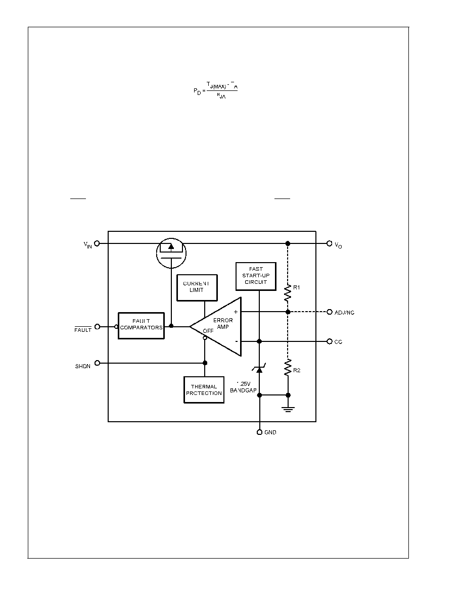
Functional Block Diagram
20036913
LP3982
www.national.com
3
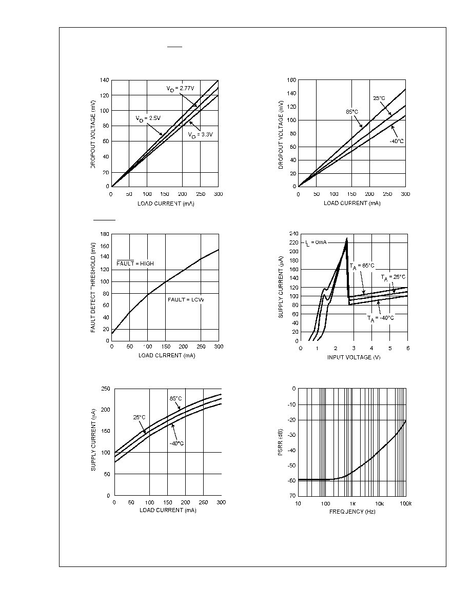
Typical Performance Characteristics
Unless otherwise specified, V
IN
= V
O
+ 0.5V, C
IN
= C
OUT
=
2.2µF, C
CC
= 33nF, T
J
= 25∞C, V
SHDN
= V
IN
.
Dropout Voltage vs. Load Current
(For Different Output Voltages)
Dropout Voltage vs. Load Current
(For Different Output Temperatures)
20036903
20036927
FAULT Detect Threshold vs. Load Current
Supply Current vs. Input Voltage
20036928
20036929
Supply Current vs. Load Current
Power Supply Rejection Ratio vs. Frequency
20036930
20036904
LP3982
www.national.com
4
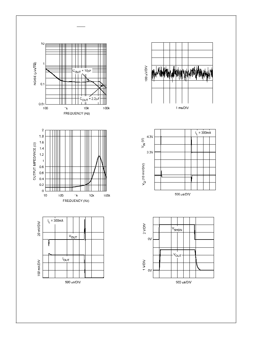
Typical Performance Characteristics
Unless otherwise specified, V
IN
= V
O
+ 0.5V, C
IN
= C
OUT
=
2.2µF, C
CC
= 33nF, T
J
= 25∞C, V
SHDN
= V
IN
. (Continued)
Output Noise Spectral Density
Output Noise (10Hz to 100kHz)
20036905
20036906
Output Impedance vs. Frequency
Line Transient Response
20036907
20036908
Load Transient
Shutdown Response
20036909
20036910
LP3982
www.national.com
5