LP3983
Micropower, Low Quiescent Current, CMOS Voltage
Regulator in micro SMD Package
General Description
The LP3983 is a fixed voltage low current regulator.
The LP3983 is ideally suited to standby type applications in
battery powered equipment, it allows the lifetime of the bat-
tery to be maximized. The device can be controlled via an
Enable(disable) control and can thus be used by the system
to further extend the battery lifetime by reducing the power
consumption to virtually zero.
Performance is specified for a -40∞C to 125∞C temperature
range.
For output voltages other than those stated and alternative
package options, please contact your local NSC sales office.
Features
n
Miniature 5 pin package
n
Logic Controlled Enable
n
No Noise Bypass Capacitor Required
n
Stable with Low ESR Ceramic Capacitors
n
Fast turn ON
n
Short Circuit Protection
Package
n
Tiny 5 Pin micro SMD
828µm by 1387µm
Key Specifications
n
Input Voltage Range
2.5 to 6.0V
n
Output Voltages
1.6, 1.8, & 2.5
n
Output Current
5mA
n
Output Capacitors
1µF Low ESR
n
Virtually Zero I
Q
(Disabled)
1.0µA
n
Low I
Q
(Enabled)
14µA
n
PSRR
10dB
n
Fast Start Up
170µs
Applications
n
GSM Portable Phones
n
CDMA Cellular Handsets
n
Bluetooth Devices
n
Portable Information Appliances
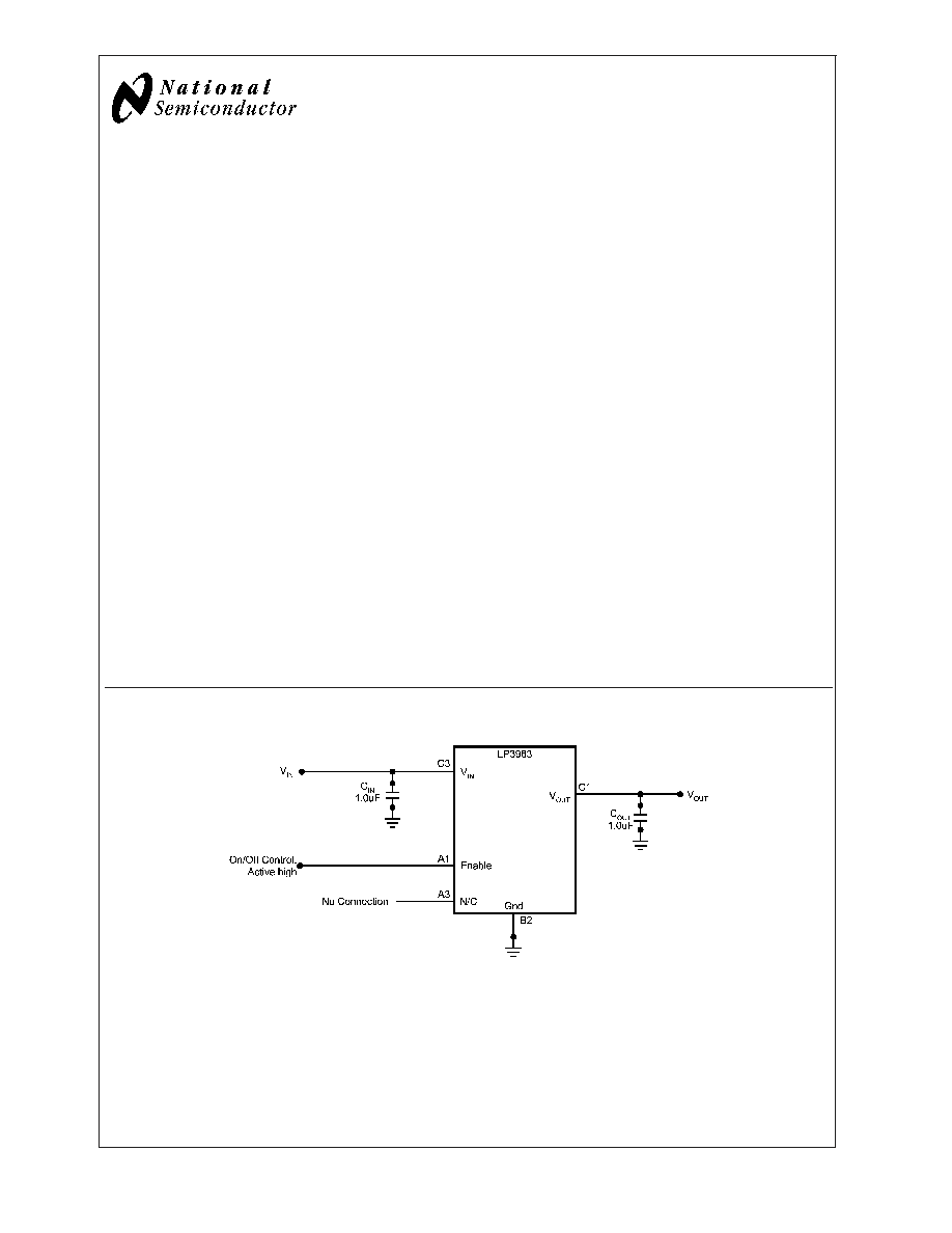
Typical Application Circuit
20057601
May 2003
LP3983
Micropower
,
Low
Quiescent
Current,
CMOS
V
oltage
Regulator
in
micro
SMD
Package
© 2003 National Semiconductor Corporation
DS200576
www.national.com
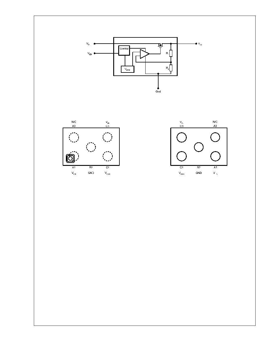
Block Diagram
LP3983
20057602
Connection Diagrams
5 Pin micro SMD Package
5 Pin micro SMD Package
20057603
Top View
See NS Package Number TLA05
20057604
Bottom View
See NS Package Number TLA05
LP3983
www.national.com
2

Pin Descriptions
Name
Pin No.
Name and Function
V
EN
A1
Enable Input Logic,
Enables regulator when
1.2V. Disables regulator when 0.5V
GND
B2
Common Ground
V
OUT
C1
Voltage Output. Connect this Output to the Load Circuit.
V
IN
C3
Unregulated supply Input.
N/C
A3
No Connection. There should be no electrical connection made to
this pin.
Ordering Information
TL refers as 0.300mm bump size with package height of 0.6mm
Output
Voltage (V)
Grade
LP3983 Supplied as 250
Units, Tape and Reel
LP3983 Supplied as 3000
Units, Tape and Reel
1.6
STD
LP3983ITL-1.6
LP3983ITLX-1.6
1.8
STD
LP3983ITL-1.8
LP3983ITLX-1.8
2.5
STD
LP3983ITL-2.5
LP3983ITLX-2.5
* Please contact National Semiconductor for availability
LP3983
www.national.com
3
Absolute Maximum Ratings
(Notes 1,
2)
If Military/Aerospace specified devices are required,
please contact the National Semiconductor Sales Office/
Distributors for availability and specifications.
V
IN
-0.3 to 6.5V
V
EN
-0.3 to (V
IN
+ 0.3V) to
6.5V(max)
V
OUT
-0.3V to(V
IN
+ 0.3V) to
6.5V(max)
Junction Temperature
150∞C
Storage Temperature
-65∞C to +150∞C
Pad Temperature
(Soldering, 10 sec.)
265∞C
ESD (Note 4)
Human Body Model
2KV
Machine Model
100V
Operating Ratings
(Notes 1, 2)
V
IN
(Note 9)
V
IN(MIN)
to 6V
V
EN
,
0 to 6.0V
Recommended Load Current
0 to 5mA
Junction Temperature
-40∞C to +125∞C
Ambient Temperature
(Note 3)
-40∞C to +119∞C
Thermal Properties
(Note 3)
Junction to Ambient Thermal
Resistance (
JA
)
255∞C/W
Electrical Characteristics
Unless otherwise specified: V
EN
= 1.8V,V
IN
= V
OUT(nom)
+ 1.0V, C
IN
= 1.0 µF, I
OUT
= 1.0mA, C
OUT
= 1.0 µF. Typical values
and limits appearing in standard typeface are for T
J
= 25∞C. Limits appearing in boldface type apply over the entire junction
temperature range for operation, -40∞C to +125∞C. (Note 10) (Note 11)
Symbol
Parameter
Conditions
Typ
Limit
Units
Min
Max
V
OUT
Output Voltage
Tolerance
I
OUT
= 0mA to 5mA
-55
+55
mV from
V
OUT(nom)
-96
+96
- 6
+6
% of
V
OUT(nom)
PSRR
Power Supply Rejection
Ratio
V
IN
= V
OUT(nom)
+ 1V,
f
10 kHz, I
OUT
= 1mA
10
dB
I
Q
Quiescent Current
I
OUT
= 50µA, V
IN
= 4.2V
14
21
µA
V
EN
= 0.4V, V
IN
= 4.2V
1
3
I
SC
Short Circuit Current
Limit (Note 7)
Output Grounded
28
35
mA
I
OUT
Maximum Output
Current
(Note 6)
5
mA
Logic Control Characteristics
I
EN
Maximum Input Current
at V
EN
input
V
EN
= 0.4 and V
IN
= 6.0V
0.02
µA
V
IL
Logic Low Input
Threshold
V
IN
= V
IN(MIN)
to 6.0V
0.5
V
V
IH
Logic High Input
Threshold
V
IN
= V
IN(MIN)
to 6.0V
1.2
V
Timing Characteristics
T
ON
Turn on Time(Note 7)
(Note 8)
170
250
µs
Note 1: Absolute Maximum Ratings are limits beyond which damage to the device may occur. Operating Ratings are conditions under which operation of the device
is guaranteed. Operating Ratings do not imply guaranteed performance limits. For guaranteed performance limits and associated test conditions, see the Electrical
Characteristics tables.
Note 2: All voltages are with respect to the potential at the GND pin.
Note 3: The maximum ambient temperature (T
A(max)
) is dependant on the maximum operating junction temperature (T
J(max-op)
= 125∞C), the maximum power
dissipation of the device in te application (P
D(max)
), and the junction to ambient thermal resistance of the part/package in the application (
JA
), as given by the
following equation: T
A(max)
= T
J(max-op)
- (
JA
x P
D(max)
).
Note 4: The human body model is 100pF discharged through a 1.5k
resistor into each pin. The machine model is a 200pF capacitor discharged directly into each
pin.
Note 5: Junction to ambient thermal resistance is dependant on the application and board layout. In applications where high maximum power dissipation is possible,
special care must be paid to thermal dissipation issues in board design.
Note 6: The device maintains the regulated output voltage without load.
LP3983
www.national.com
4
Electrical Characteristics
(Continued)
Note 7: This electrical specification is guaranteed by design.
Note 8: Time from V
EN
= 1.2V to V
OUT
= 95% of V
OUT(NOM)
Note 9: The minimum V
IN
is dependant on the device output option.
For V
OUT(NOM)
2.7V, V
IN(MIN)
will equal 2.5V. For V
OUT(NOM)
>
2.7V, V
IN(MIN)
will equal V
OUT(NOM)
+ 200mV.
Note 10: All limits are guaranteed. All electrical characteristics having room-temperature limits are tested during production with T
J
= 25∞C or correlated using
Statistical Quality Control methods. Operation over the temperature specification is guaranteed by correlating the electrical characteristics to process and
temperature variations and applying statistical process control.
Note 11: The target output voltage which is labelled V
OUT(NOM)
is the desired voltage option.
Output Capacitor, Recommended Specifications
Symbol
Parameter
Conditions
Value
Limit
Units
Min
Max
C
o
Output Capacitor
Capacitance(Note 12)
1.0
0.75
µF
ESR
5
500
m
Note 12: The capacitor tolerance should be
±
25% or better over the temperature range. Capacitor types recommended are X7R, Y5V, and Z5U.
LP3983
www.national.com
5