LP3984
Micropower, 150mA Ultra Low-Dropout CMOS Voltage
Regulator in Subminiature 4-I/O micro SMD Package
General Description
The LP3984 is designed for portable and wireless applica-
tions with demanding performance and space requirements.
The LP3984's performance is optimized for battery powered
systems to deliver extremely low dropout voltage and low
quiescent current. Regulator ground current increases only
slightly in dropout, further prolonging the battery life.
Power supply rejection is better than 60 dB at low frequen-
cies and starts to roll off at 10 kHz. High power supply
rejection is maintained down to lower input voltage levels
common to battery operated circuits.
The device is ideal for mobile phone and similar battery
powered wireless applications. It provides up to 150 mA,
from a 2.5V to 6V input, consuming less than 1.2µA in
disable mode and has fast turn-on time less than 20µs.
The LP3984 is available in micro SMD and 5 pin SOT-23
package. Performance is specified for -40∞C to +125∞C
temperature range and is available in 1.5V, 1.8V, 2.0V, and
3.1V output voltages. For other output voltage options from
1.5V to 3.5V, please contact National Semiconductor sales
office.
Key Specifications
n
2.5 to 6.0V input range
n
150mA guaranteed output
n
60dB PSRR at 1kHz, 40dB at 10kHz
@
3.1V
IN
n
1.2µA quiescent current when shut down
n
Fast Turn-On time: 20 µs (typ.)
n
75mV typ dropout with 150mA load
n
-40 to +125∞C junction temperature range for operation
n
1.5V, 1.8V, 2.0V, and 3.1V
Features
n
Miniature 4-I/O micro SMD and SOT-23-5 package
n
Logic controlled enable
n
Stable with tantalum capacitors
n
1 µF Tantalum output capacitor
n
Fast turn-on
n
Thermal shutdown and short-circuit current limit
Applications
n
CDMA cellular handsets
n
Wideband CDMA cellular handsets
n
GSM cellular handsets
n
Portable information appliances
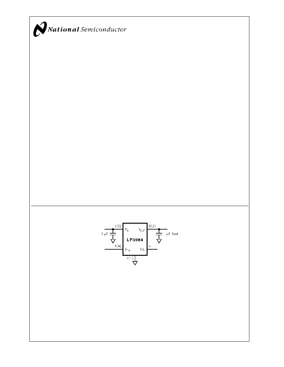
Typical Application Circuit
20020402
Note: Pin Numbers in parenthesis indicate micro SMD package.
November 2001
LP3984
Micropower
,
150mA
Ultra
Low-Dropout
CMOS
V
oltage
Regulator
in
Subminiature
4-I/O
micro
SMD
Package
© 2001 National Semiconductor Corporation
DS200204
www.national.com
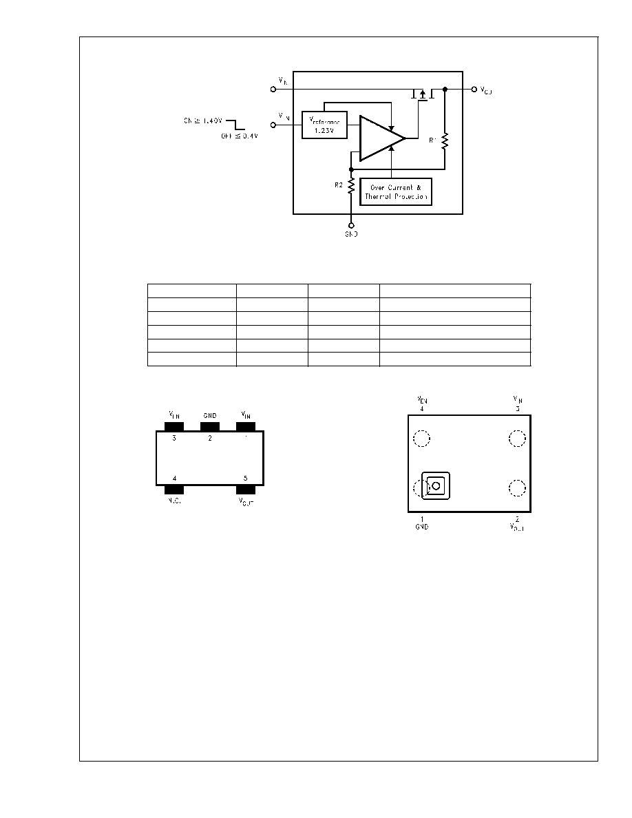
Block Diagram
20020401
Pin Descriptions
Name
µSMD
SOT
Function
V
EN
4
3
Enable Input Logic, Enable High
GND
1
2
Common Ground
V
OUT
2
5
Output Voltage of the LDO
V
IN
3
1
Input Voltage of the LDO
N.C.
4
No Connection
Connection Diagrams
SOT-23-5 Package
20020407
Top View
See NS Package Number MF05A
micro SMD, 4 Bump Package
20020470
Top View
See NS Package Number BPA04
Note: The actual physical placement of the package marking will vary from
part to part. The package marking will designate the date code. Package
marking does not correlate to device type in any way.
LP3984
www.national.com
2
Ordering Information
For micro SMD Package
Output
Voltage (V)
Grade
LP3984 Supplied as 250
Units, Tape and Reel
LP3984 Supplied as 3000
Units, Tape and Reel
1.5
STD
LP3984IBP-1.5
LP3984IBPX-1.5
1.8
STD
LP3984IBP-1.8
LP3984IBPX-1.8
2.0
STD
LP3984IBP-2.0
LP3984IBPX-2.0
3.1
STD
LP3984IBP-3.1
LP3984IBPX-3.1
For SOT Package
Output
Voltage (V)
Grade
LP3984 Supplied as 1000
Units, Tape and Reel
LP3984 Supplied as 3000
Units, Tape and Reel
Package Marking
1.5
STD
LP3984IMF-1.5
LP3984IMFX-1.5
LEAB
1.8
STD
LP3984IMF-1.8
LP3984IMFX-1.8
LEBB
2.0
STD
LP3984IMF-2.0
LP3984IMFX-2.0
LECB
3.1
STD
LP3984IMF-3.1
LP3984IMFX-3.1
LEDB
LP3984
www.national.com
3
Absolute Maximum Ratings
(Notes 1,
2)
If Military/Aerospace specified devices are required,
please contact the National Semiconductor Sales Office/
Distributors for availability and specifications.
V
IN
,V
OUT
, V
EN
-0.3 to 6.5V
Junction Temperature
150∞C
Storage Temperature
-65∞C to +150∞C
Lead Temp. (Note 3)
235∞C
Pad Temp. (Note 3)
235∞C
Power Dissipation (Note 4)
JA
(SOT23-5)
JA
(micro SMD)
220∞C/W
340∞C/W
Maximum Power Dissipation
SOT23-5
Micro SMD
364mW
235mW
ESD Rating(Note 5)
Human Body Model
Machine Model
2kV
200V
Operating Ratings
(Notes 1, 2)
V
IN
2.5 to 6V
V
EN
0 to (V
IN
+ 0.3V)
Junction Temperature
-40∞C to +125∞C
Maximum Power Dissipation (Note 6)
SOT23-5
micro SMD
250mW
160mW
Electrical Characteristics
Unless otherwise specified: V
IN
= 2.5V for 1.5, 1.8, & 2.0V options, V
IN
= V
OUT
+ 0.5 for output options higher than 2.5V, C
IN
=
1 µF, I
OUT
= 1mA, C
OUT
= 1 µF, tantalum. Typical values and limits appearing in standard typeface are for T
J
= 25∞C. Limits
appearing in boldface type apply over the entire junction temperature range for operation, -40∞C to +125∞C. (Note 7) (Note 8)
Symbol
Parameter
Conditions
Typ
Limit
Units
Min
Max
V
OUT
Output Voltage
Tolerance
-1.2
-2.0
1.2
2.0
% of
V
OUT(nom)
Line Regulation Error
V
IN
= 2.5V to 4.5V for 1.5, 1.8, 2.0V
options
V
IN
= (V
OUT
+ 0.5V) to 4.5V for
Voltage options higher than 2.5V
0.05
-0.15
0.15
%/V
Load Regulation Error
(Note 9)
I
OUT
= 1 mA to 150 mA
LP3984IM5 (SOT23-5)
0.002
0.005
%/mA
LP3984IBP (micro SMD)
0.0009
0.002
PSRR
Power Supply Rejection Ratio
V
IN
= V
OUT(nom)
+ 0.2V,
f = 1 kHz,
I
OUT
= 50 mA (
Figure 2)
60
dB
V
IN
= V
OUT(nom)
+ 0.2V,
f = 10 kHz,
I
OUT
= 50 mA (
Figure 2)
40
I
Q
Quiescent Current
V
EN
= 1.4V, I
OUT
= 0 mA
80
125
µA
V
EN
= 1.4V, I
OUT
= 0 to 150 mA
110
150
V
EN
= 0.4V
0.005
1.2
Dropout Voltage (Note 10)
I
OUT
= 1 mA
0.6
2.5
mV
I
OUT
= 50 mA
25
40
I
OUT
= 100 mA
50
80
I
OUT
= 150 mA
75
120
I
SC
Short Circuit Current Limit
Output Grounded
(Steady State)
600
mA
I
OUT(PK)
Peak Output Current
V
OUT
V
OUT(nom)
- 5%
600
300
mA
T
ON
Turn-On Time
(Note 11)
20
µs
e
n
Output Noise Voltage
BW = 10 Hz to 100 kHz,
C
OUT
= 1µF tant.
90
µVrms
I
EN
Maximum Input Current at EN
V
EN
= 0.4 and V
IN
= 6.0
±
1
nA
LP3984
www.national.com
4
Electrical Characteristics
(Continued)
Unless otherwise specified: V
IN
= 2.5V for 1.5, 1.8, & 2.0V options, V
IN
= V
OUT
+ 0.5 for output options higher than 2.5V, C
IN
=
1 µF, I
OUT
= 1mA, C
OUT
= 1 µF, tantalum. Typical values and limits appearing in standard typeface are for T
J
= 25∞C. Limits
appearing in boldface type apply over the entire junction temperature range for operation, -40∞C to +125∞C. (Note 7) (Note 8)
Symbol
Parameter
Conditions
Typ
Limit
Units
Min
Max
V
IL
Maximum Low Level Input
Voltage at EN
V
IN
= 2.5 to 6.0V
0.4
V
V
IH
Minimum High Level Input
Voltage at EN
V
IN
= 2.5 to 6.0V
1.4
V
C
OUT
Output Capacitor
Capacitance
1
22
µF
ESR
2
10
TSD
Thermal Shutdown Temperature
160
∞C
Thermal Shutdown Hysteresis
20
∞C
Note 1: Absolute Maximum Ratings are limits beyond which damage to the device may occur. Operating Ratings are conditions under which operation of the device
is guaranteed. Operating Ratings do not imply guaranteed performance limits. For guaranteed performance limits and associated test conditions, see the Electrical
Characteristics tables.
Note 2: All voltages are with respect to the potential at the GND pin.
Note 3: Additional information on lead temperature and pad temperature can be found in National Semiconductor Application Note (AN-1112).
Note 4: The
Absolute
Maximum
power
dissipation
depends
on
the
ambient
temperature
and
can
be
calculated
using
the
formula:
P
D
= (T
J
- T
A
)/
JA
,
where T
J
is the junction temperature, T
A
is the ambient temperature, and
JA
is the junction-to-ambient thermal resistance. The 364mW rating for SOT23-5
appearing under Absolute Maximum Ratings results from substituting the Absolute Maximum junction temperature, 150∞C, for T
J
, 70∞C for T
A
, and 220∞C/W for
JA
.
More power can be dissipated safely at ambient temperatures below 70∞C . Less power can be dissipated safely at ambient temperatures above 70∞C. The Absolute
Maximum power dissipation for SOT23-5 can be increased by 4.5mW for each degree below 70∞C, and it must be derated by 4.5mW for each degree above 70∞C.
Note 5: The human body model is 100pF discharged through 1.5k
resistor into each pin. The machine model is a 200 pF capacitor discharged directly into each
pin.
Note 6: Like the Absolute Maximum power dissipation, the maximum power dissipation for operation depends on the ambient temperature. The 250mW rating for
SOT23-5 appearing under Operating Ratings results from substituting the maximum junction temperature for operation, 125∞C, for T
J
, 70∞C for T
A
, and 220∞C/W for
JA
into (Note 4) above. More power can be dissipated at ambient temperatures below 70∞C . Less power can be dissipated at ambient temperatures above 70∞C.
The maximum power dissipation for operation can be increased by 4.5mW for each degree below 70∞C, and it must be derated by 4.5mW for each degree above
70∞C.
Note 7: All limits are guaranteed. All electrical characteristics having room-temperature limits are tested during production with T
J
= 25∞C or correlated using
Statistical Quality Control (SQC) methods. All hot and cold limits are guaranteed by correlating the electrical characteristics to process and temperature variations
and applying statistical process control.
Note 8: The target output voltage, which is labeled V
OUT(nom)
, is the desired voltage option.
Note 9: An increase in the load current results in a slight decrease in the output voltage and vice versa.
Note 10: Dropout voltage is the input-to-output voltage difference at which the output voltage is 100mV below its nominal value. This specification does not apply
for input voltages below 2.5V.
Note 11: Turn-on time is time measured between the enable input just exceeding V
IH
and the output voltage just reaching 95% of its nominal value.
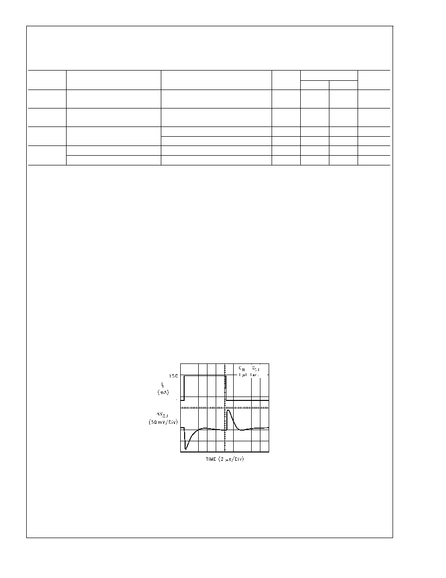
20020408
FIGURE 1. Output AC Line Regulation Input Perturbation
LP3984
www.national.com
5