LP3986
Dual Micropower 150 mA Ultra Low-Dropout CMOS
Voltage Regulators in micro SMD Package
General Description
The LP3986 is a 150 mA dual low dropout regulator de-
signed for portable and wireless applications with demand-
ing performance and board space requirements.
The LP3986 is stable with a small 1 µF
±
30% ceramic output
capacitor requiring smallest possible board space.
The LP3986's performance is optimized for battery powered
systems to deliver ultra low noise, extremely low dropout
voltage and low quiescent current independent of load cur-
rent. Regulator ground current increases very slightly in
dropout, further prolonging the battery life. Optional external
bypass capacitor reduces the output noise further without
slowing down the load transient response. Fast start-up time
is achieved by utilizing a speed-up circuit that actively pre-
charges the bypass capacitor. Power supply rejection is
better than 60 dB at low frequencies and 55 dB at 10 kHz.
High power supply rejection is maintained at low input volt-
age levels common to battery operated circuits.
The LP3986 is available in a micro SMD package. Perfor-
mance is specified for a -40∞C to +125∞C temperature
range. For single LDO applications, please refer to the
LP3985 datasheet.
Features
n
Miniature 8-I/O micro SMD package
n
Stable with 1µF ceramic and high quality tantalum
output capacitors
n
Fast turn-on
n
Two independent regulators
n
Logic controlled enable
n
Over current and thermal protection
Key Specifications
n
Guaranteed 150 mA output current per regulator
n
1nA typical quiescent current when both regulators in
shutdown mode
n
60 mV typical dropout voltage at 150 mA output current
n
115 µA typical ground current
n
40 µV typical output noise
n
200 µs fast turn-on circuit
n
-40∞C to +125∞C junction temperature
Applications
n
CDMA cellular handsets
n
GSM cellular handsets
n
Portable information appliances
n
Portable battery applications
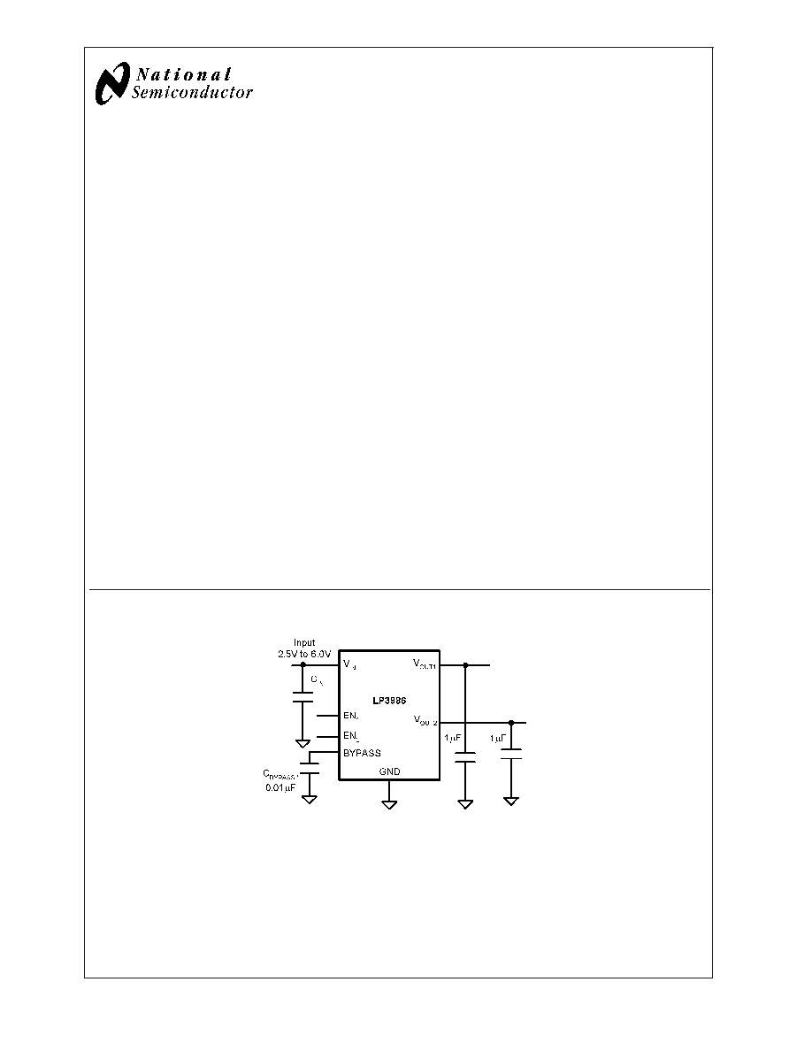
Typical Application Circuit
20003401
May 2003
LP3986
Dual
Micropower
150
mA
Ultra
Low-Dropout
CMOS
V
oltage
Regulators
in
micro
SMD
Package
© 2003 National Semiconductor Corporation
DS200034
www.national.com
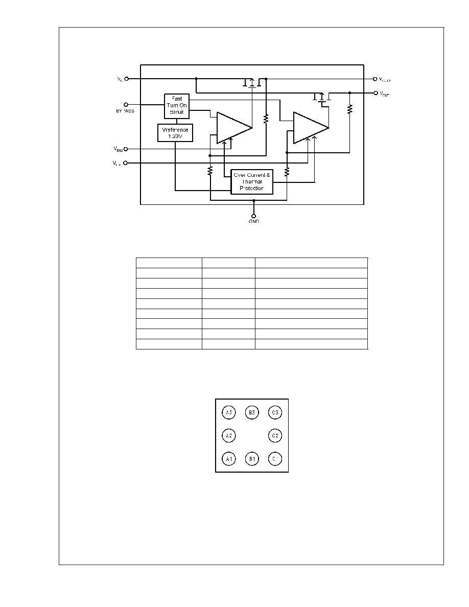
Block Diagram
LP3986
20003402
Pin Description
Name
*micro SMD
Function
V
OUT2
A1
Output Voltage of the second LDO
EN
2
B1
Enable input for the second LDO
BYPASS
C1
Bypass capacitor for the bandgap
GND
C2
Common ground
GND
C3
Common ground
EN
1
B3
Enable input for the first LDO
V
OUT1
A3
Output Voltage of the first LDO
V
IN
A2
Common input for both LDOs
* Note: The pin numbering scheme for the micro SMD package was revised in April 2002 to conform to JEDEC standard. Only the pin
numbers were revised. No changes to the physical location of the inputs/outputs were made. For reference purposes, the obsolete
numbering scheme had V
OUT2
as pin 1, EN
2
as pin 2, BYPASS as pin 3, GND as pins 4 and 5, EN
1
as pin 6, V
OUT1
as pin 7, and V
IN
as pin 8.
Connection Diagram
20003404
Top View
8 Bump micro SMD Package
See NS Package Number BLA08
LP3986
www.national.com
2
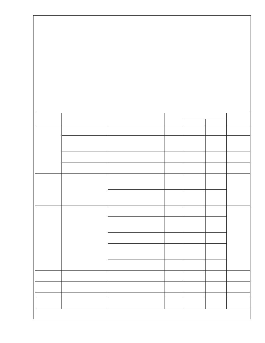
Absolute Maximum Ratings
(Notes 1,
2)
If Military/Aerospace specified devices are required,
please contact the National Semiconductor Sales Office/
Distributors for availability and specifications.
V
IN
, V
EN
-0.3 to 6.5V
V
OUT
-0.3 to (V
IN
+0.3V)
6.5V
Junction Temperature
150∞C
Storage Temperature
-65∞C to +150∞C
Pad Temp. (Note 3)
235∞C
Maximum Power Dissipation
(Note 4)
364mW
ESD Rating (Note 5)
Human Body Model
Machine Model
2kV
200V
Operating Ratings
(Notes 1, 2)
V
IN
2.5 to 6V
V
EN
0 to (V
IN
+ 0.3V)
6V
Junction Temperature
-40∞C to +125∞C
Thermal Resistance
JA
220∞C/W
Maximum Power Dissipation (Note 6)
250mW
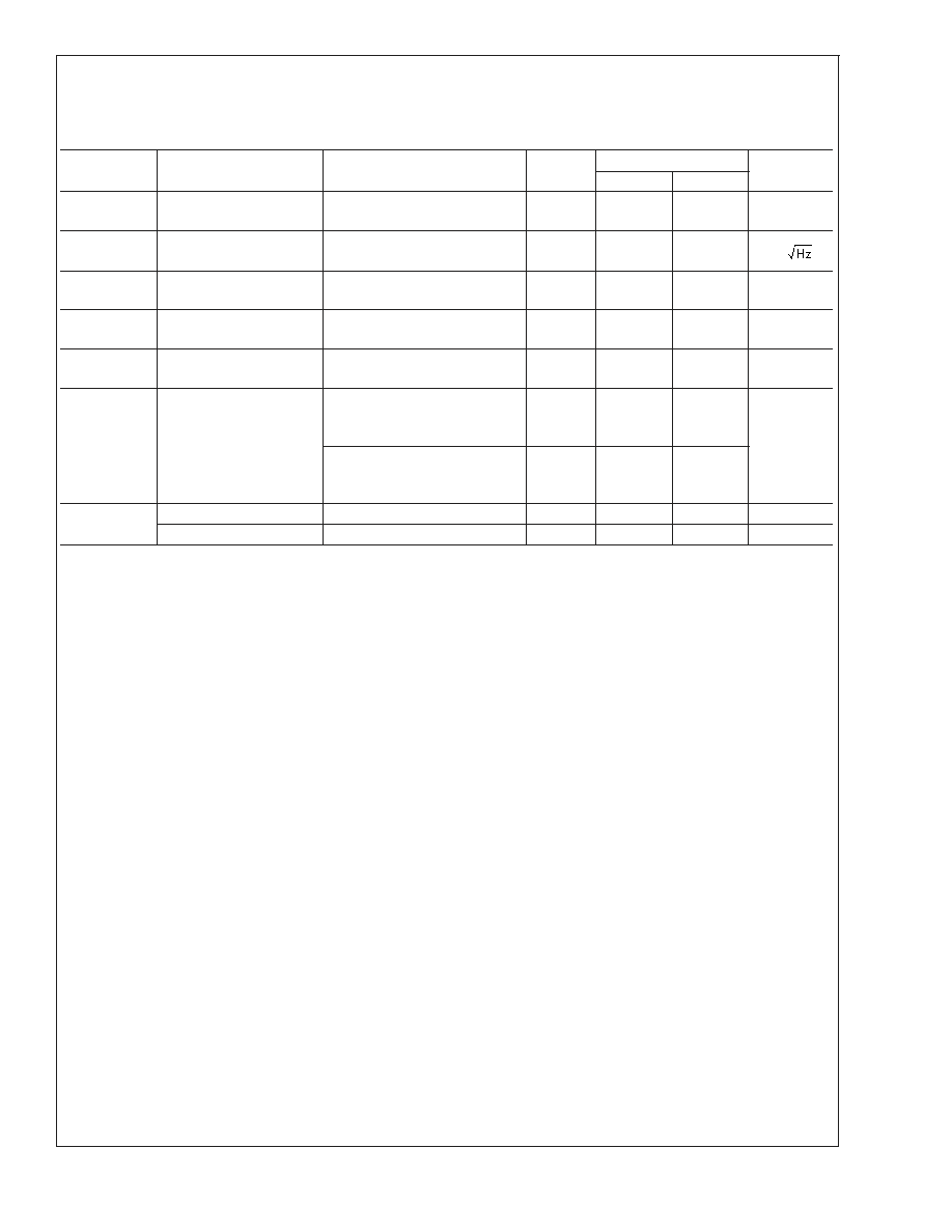
Electrical Characteristics
Unless otherwise specified: V
IN
= V
OUT(nom)
+ 0.5V, C
IN
= 1 µF, I
OUT
= 1mA, C
OUT
= 1 µF, C
BYPASS
= 0.01µF. Typical values
and limits appearing in standard typeface are for T
J
= 25∞C. Limits appearing in boldface type apply over the entire junction
temperature range for operation, -40∞C to +125∞C. (Note 7) (Note 8)
Symbol
Parameter
Conditions
Typ
Limit
Units
Min
Max
V
OUT
Output Voltage
Tolerance
I
OUT
= 1mA
-2.5
-3.0
2.5
3.0
% of
V
OUT(nom)
Line Regulation Error
(Note 9)
V
IN
= (V
OUT(nom)
+ 0.5V) to
6.0V,
I
OUT
= 1 mA
0.006
0.092
0.128
%/V
Load Regulation Error
(Note 10)
I
OUT
= 1mA to 150 mA
0.003
0.006
0.01
%/mA
Output AC Line
Regulation
V
IN
= V
OUT(nom)
+ 1V,
I
OUT
= 150 mA (Figure 1)
1.5
mV
P-P
PSRR
Power Supply Rejection
Ratio
V
IN
= 3.1V,
f = 1 kHz,
I
OUT
= 50 mA (Figure 2)
60
dB
V
IN
= 3.1V,
f = 10 kHz,
I
OUT
= 50 mA (Figure 2)
50
I
Q
Quiescent Current
Both Regulators ON
V
EN
= 1.4V, I
OUT
= 0 mA
115
200
µA
Both Regulators ON
V
EN
= 1.4V, I
OUT
= 0 to 150
mA
220
320
One Regulator ON
V
EN
= 1.4V I
OUT
= 0 mA
75
130
One Regulator ON
V
EN
= 1.4V I
OUT
= 0 to 150
mA
130
200
V
EN
= 0.4V, Both Regulators
OFF (shutdown)
0.001
2
4
Dropout Voltage
(Note 11)
I
OUT
= 1 mA
I
OUT
= 150 mA
0.4
60
2
100
mV
I
SC
Short Circuit Current
Limit
Output Grounded
600
mA
I
OUT(PK)
Peak Output Current
V
OUT
V
OUT(nom)
- 5%
500
300
mA
T
ON
Turn-On Time
(Note 12)
C
BYPASS
= 0.01 µF
200
µs
LP3986
www.national.com
4
Electrical Characteristics
(Continued)
Unless otherwise specified: V
IN
= V
OUT(nom)
+ 0.5V, C
IN
= 1 µF, I
OUT
= 1mA, C
OUT
= 1 µF, C
BYPASS
= 0.01µF. Typical values
and limits appearing in standard typeface are for T
J
= 25∞C. Limits appearing in boldface type apply over the entire junction
temperature range for operation, -40∞C to +125∞C. (Note 7) (Note 8)
Symbol
Parameter
Conditions
Typ
Limit
Units
Min
Max
e
n
Output Noise Voltage
BW = 10 Hz to 100 kHz,
C
OUT
= 1µF
40
µVrms
n(1/f)
Output Noise Density
f = 120 Hz,
C
OUT
= 1µF
1
µV/
I
EN
Maximum Input Current
at EN
V
EN
= 0.4 and V
IN
= 6V
±
10
nA
V
IL
Maximum Low Level
Input Voltage at EN
V
IN
= 2.5 to 6V
0.4
V
V
IH
Minimum High Level
Input Voltage at EN
V
IN
= 2.5 to 6V
1.4
V
Xtalk
Crosstalk Rejection
I
Load1
= 150 mA at 1KHz rate
I
Load2
= 1 mA
V
OUT2
/
V
OUT1
-60
dB
I
Load2
= 150 mA at 1KHz rate
I
Load1
= 1 mA
V
OUT2
/
V
OUT1
-60
C
OUT
Capacitance
(Note 13)
1
22
µF
ESR
(Note 14)
5
500
m
Note 1: Absolute Maximum Ratings are limits beyond which damage to the device may occur. Operating Ratings are conditions under which operation of the device
is guaranteed. Operating Ratings do not imply guaranteed performance limits. For guaranteed performance limits and associated test conditions, see the Electrical
Characteristics tables.
Note 2: All voltages are with respect to the potential at the GND pin.
Note 3: Additional information on pad temperature can be found in National Semiconductor Application Note (AN-1112).
Note 4: The Absolute Maximum power dissipation depends on the ambient temperature and can be calculated using the formula:
P
D
= (T
J
- T
A
)/
JA
,
Where T
J
is the junction temperature, T
A
is the ambient temperature, and
JA
is the junction-to-ambient thermal resistance. The 364mW rating appearing under
Absolute Maximum Ratings results from substituting the Absolute Maximum junction temperature, 150∞C, for T
J
, 70∞C for T
A
, and 220∞C/W for
JA
. More power can
be dissipated safely at ambient temperatures below 70∞C . Less power can be dissipated safely at ambient temperatures above 70∞C. The Absolute Maximum power
dissipation can be increased by 4.5mW for each degree below 70∞C, and it must be derated by 4.5mW for each degree above 70∞C.
Note 5: The human body model is 100pF discharged through a 1.5k
resistor into each pin. The machine model is a 200pF capacitor discharged directly into each
pin.
Note 6: Like the Absolute Maximum power dissipation, the maximum power dissipation for operation depends on the ambient temperature. The 250mW rating
appearing under Operating Ratings results from substituting the maximum junction temperature for operation, 125∞C, for T
J
, 70∞C for T
A
, and 220∞C/W for
JA
into
(1) above. More power can be dissipated at ambient temperatures below 70∞C . Less power can be dissipated at ambient temperatures above 70∞C. The maximum
power dissipation for operation can be increased by 4.5mW for each degree below 70∞C, and it must be derated by 4.5mW for each degree above 70∞C.
Note 7: All limits are guaranteed. All electrical characteristics having room temperature limits are tested during production with T
J
= 25∞C or correlated using
Statistical Quality Control (SQC) methods. All hot and cold limits are guaranteed by correlating the electrical characteristics to process and temperature variations
and applying statistical process control.
Note 8: The target output voltage, which is labeled V
OUT(nom)
, is the desired voltage option.
Note 9: The output voltage changes slightly with line voltage. An increase in the line voltage results in a slight increase in the output voltage and vice versa.
Note 10: The output voltage changes slightly with load current. An increase in the load current results in a slight decrease in the output voltage and vice versa.
Note 11: Dropout voltage is the input-to-output voltage difference at which the output voltage is 100mV below its nominal value.
Note 12: Turn-on time is that between the enable input just exceeding V
IH
and the output voltage just reaching 95% of its nominal value.
Note 13: Range of capacitor values for which the device will remain stable. This electrical specification is guaranteed by design.
Note 14: Range of capacitor ESR values for which the device will remain stable. This electrical specification is guaranteed by design.
LP3986
www.national.com
5