
LP3987
Micropower micro SMD 150 mA Ultra Low-Dropout
CMOS Voltage Regulators with sleep MODE
General Description
The LP3987 is a 150mA fixed output voltage regulator with
very low dropout voltage designed specially to meet require-
ments of battery-powered applications. The additional sleep
MODE feature will reduce current consumption during
standby operation to prolong the usage of battery.
Dropout Voltage: 100mV maximum dropout with 150mA
load.
Shutdown: Less than 1µA quiescent current.
Sleep Mode: Typically 14µA quiescent current during sleep
MODE to reduce battery consumption.
Enhanced Stability: The LP3987 is stable with minimum
1µF
±
20% low ESR ceramic output capacitor as low as 5m
and high quality tantalum capacitors.
The LP3987 is available in thin and thick 5 Bump micro SMD
package. Performance is specified for -40∞C to 125∞C.
This device is available with output voltage options of 2.6V,
2.8V, & 2.85V. For other voltage options, please contact
National Semiconductor Corporation.
Features
n
Miniature 5-I/O micro SMD package
n
Stable with ceramic and high quality tantalum output
capacitors
n
Logic controlled enable
n
Thermal Shutdown and short-circuit current limit
Key Specifications
n
2.7 to 6.0V input range
n
Guaranteed 150 mA output current
n
1µA quiescent current on shutdown
n
100 mV maximum dropout with 150 mA load
n
50dB PSRR at 10KHz
n
Sleep MODE features
n
Over temperature & over current protection
n
-40∞C to +125∞C junction temperature range for
operation
Applications
n
CDMA cellular handsets
n
Wideband CDMA cellular handsets
n
GSM cellular handsets
n
Portable information appliances
n
µP/DSP Power Supplies
n
Digital Cameras
n
SRAM Backup
Typical Application Circuit
20022201
February 2003
LP3987
Micropower
micro
SMD
150
mA
Ultra
Low-Dropout
CMOS
V
oltage
Regulators
with
sleep
MODE
© 2003 National Semiconductor Corporation
DS200222
www.national.com
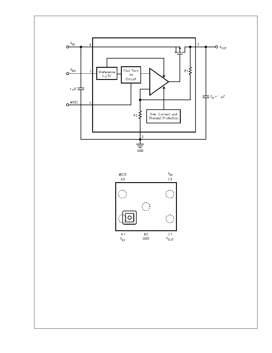
Block Diagram
LP3987
20022202
Connection Diagram
20022271
Top View
5 I/O micro SMD Package
See NS Package Number BPA05/TLA05/BLA05
LP3987
www.national.com
2
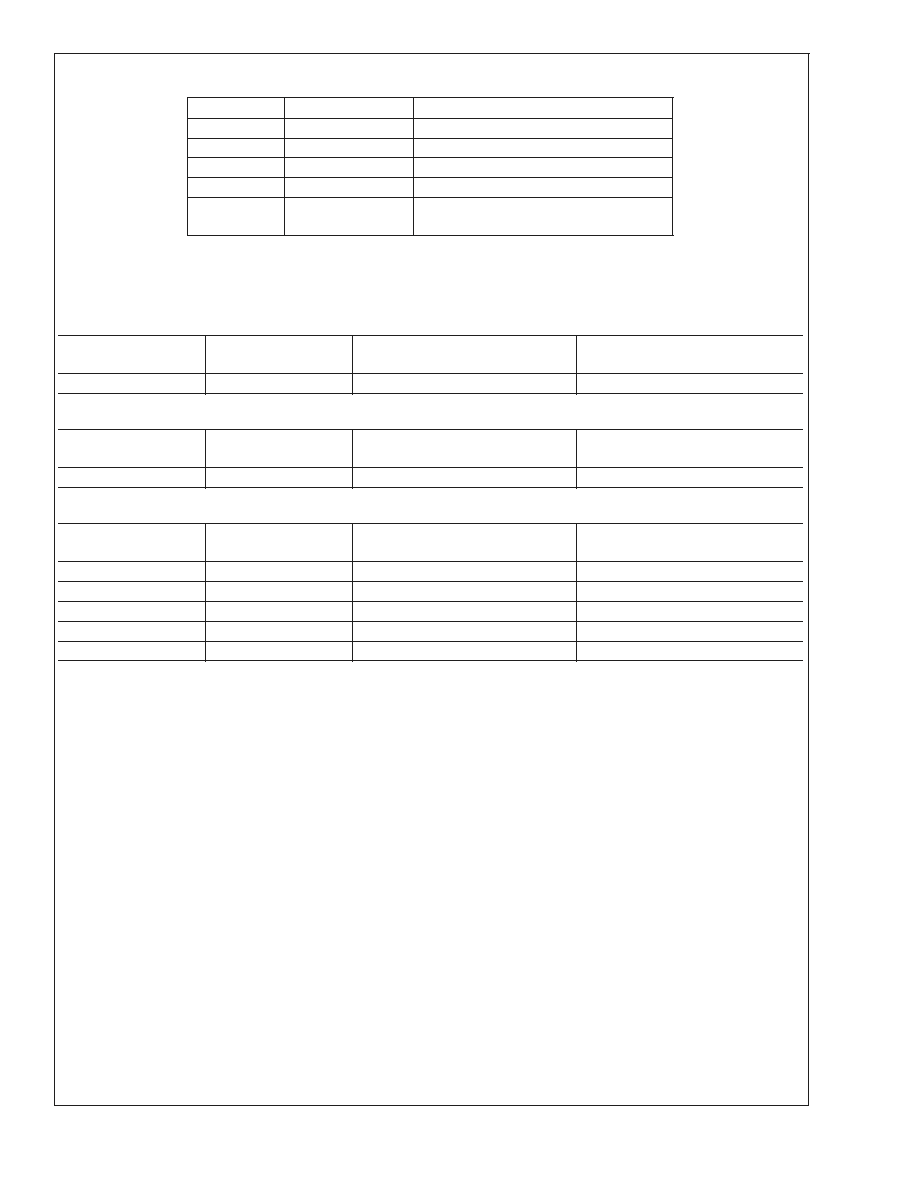
Pin Descriptions
Name
micro SMD*
Function
V
EN
A1
Enable Input Logic, Enable High
GND
B2
Common Ground
V
OUT
C1
Output voltage of the LDO
V
IN
C3
Input voltage of the LDO
MODE
A3
Power Mode Control, Active = 1, Sleep
Mode = 0
* The pin numbering scheme for the micro SMD package was revised in April, 2002 to conform to JEDEC standard. Only the pin numbers
were revised. No changes to the physical location of the inputs/outputs were made. For reference purposes, the obsolete numbering
scheme had VEN as pin 1, GND as pin 2, VOUT as pin 3, VIN as pin 4, and MODE as pin 5.
Ordering Information
BP refers to a 0.170mm bump size with package height of 0.9mm
Output
Voltage (V)
Grade
LP3987 Supplied as 250
Units, Tape and Reel
LP3987 Supplied as 3000
Units, Tape and Reel
2.85*
STD
LP3987IBP-2.85
LP3987IBPX-2.85
* Please contact National Semiconductor for availability
BL refers to a 0.300mm bump size with package height of 0.9mm
Output
Voltage (V)
Grade
LP3987 Supplied as 250
Units, Tape and Reel
LP3987 Supplied as 3000
Units, Tape and Reel
2.85
STD
LP3987IBL-2.85
LP3987IBLX-2.85
* Please contact National Semiconductor for availability
TL refers to a 0.300mm bump size with package height of 0.6mm
Output
Voltage (V)
Grade
LP3987 Supplied as 250
Units, Tape and Reel
LP3987 Supplied as 3000
Units, Tape and Reel
2.5
STD
LP3987ITL-2.5
LP3987ITLX-2.5
2.6
STD
LP3987ITL-2.6
LP3987ITLX-2.6
2.8
STD
LP3987ITL-2.8
LP3987ITLX-2.8
2.85
STD
LP3987ITL-2.85
LP3987ITLX-2.85
3.0*
STD
LP3987ITL-3.0
LP3987ITLX-3.0
* Please contact National Semiconductor for availability
LP3987
www.national.com
3
Absolute Maximum Ratings
(Notes 1,
2)
If Military/Aerospace specified devices are required,
please contact the National Semiconductor Sales Office/
Distributors for availability and specifications.
V
IN
-0.3 to 6.5V
V
EN
, V
MODE
-0.3 to 6.5V
V
OUT
-0.3V to(V
IN
+
0.3V)
6.5
Storage Temperature
-65∞C to +150∞C
ESD (Note 4)
Human Body Model
2KV
Machine Model
200V
Maximum Power Dissipation (Note 3)
JA
(micro SMD small bump)
255∞C/W
Operating Ratings
(Notes 1, 2)
V
IN
V
OUT
+ 200mV to 6V
V
EN
, V
MODE
0 to 6.0V
Junction Temperature
-40∞C to +125∞C
Maximum Power Dissipation (Note 3)
392mW at 25∞C
Electrical Characteristics
Unless otherwise specified: V
EN
= 1.8V, MODE = 1.8V, V
IN
= V
OUT(nom)
+ 0.5V, C
IN
= 1 µF, I
OUT
= 1mA, C
OUT
= 1 µF. Typical
values and limits appearing in standard typeface are for T
J
= 25∞C. Limits appearing in boldface type apply over the entire
junction temperature range for operation, -40∞C to +125∞C. (Note 10) (Note 11)
Symbol
Parameter
Conditions
Typ
Limit
Units
Min
Max
V
OUT
Output Voltage
Tolerance
I
OUT
= 1mA, 25∞C
-2
2
% of
V
OUT(nom)
I
OUT
= 1mA
-3
3
Line Regulation Error
V
IN
= (V
OUT(nom)
+ 0.5V) to
6.0V,
I
OUT
= 1 mA
-0.1
0.1
%/V
Load Regulation Error
I
OUT
= 1mA to 150 mA
0.0004
0.002
%/mA
Dropout Voltage
(Note 6)
I
OUT
= 1mA
0.4
2
mV
I
OUT
= 150mA
60
100
V
OUT(SLEEP)
Output Voltage
difference at MODE =
0V
MODE = 0V, (Note 7)
-150
+100
mV
Transient
Response
Line Transient
Response (Note 5)
MODE = 1.8V, I
LOAD
=
100mA, T
RISE
= T
FALL
=
10µS,
V
IN
= 600mV
P-P
AC Square
wave, (Note 8)
21
mVpp
Load Transient
Response (Note 5)
MODE = 1.8V, C
OUT
= 4.7µF,
T
RISE
= T
FALL
= 100nS,
V
IN
= 3.1V, 3.6V, 4.2V, (Notes
9, 12)
100
mVpk
PSRR
Power Supply Rejection
Ratio (Note 5)
V
IN
= V
OUT(nom)
+ 1V, MODE
= 1.8V, f =
<
10 kHz,
I
OUT
= 1mA
50
dB
V
IN
= V
OUT(nom)
+ 1V, MODE
= 0V, f =
<
10 kHz,
I
OUT
= 1mA
10
I
Q(ON)
Quiescent Current
MODE = 1.8V, I
OUT
= 0mA,
V
IN
= 4.2V
85
120
µA
MODE = 1.8V, I
OUT
= 150mA,
V
IN
= 4.2V
160
200
I
Q(OFF)
Quiescent Current
ENABLE = 0V, V
IN
= 4.2V
1
3
µA
I
Q(SLEEP)
Current in Standby
Mode
MODE = 0V, I
OUT
= 50µA, V
IN
= 4.2V
14
21
µA
I
SC
Short Circuit Current
Limit (Note 5)
Output Grounded
600
mA
LP3987
www.national.com
4
Electrical Characteristics
(Continued)
Unless otherwise specified: V
EN
= 1.8V, MODE = 1.8V, V
IN
= V
OUT(nom)
+ 0.5V, C
IN
= 1 µF, I
OUT
= 1mA, C
OUT
= 1 µF. Typical
values and limits appearing in standard typeface are for T
J
= 25∞C. Limits appearing in boldface type apply over the entire
junction temperature range for operation, -40∞C to +125∞C. (Note 10) (Note 11)
Symbol
Parameter
Conditions
Typ
Limit
Units
Min
Max
I
SC(SLEEP)
Short Circuit Current in
Sleep MODE
Output Grounded
28
43
mA
I
OUT(ON)
Maximum Output
Current at MODE =
1.8V
MODE = 1.8V
150
mA
I
OUT(SLEEP)
Maximum Output
Current at MODE = 0V
MODE = 0V
3
mA
e
n
Output Noise Voltage,
(Note 5)
BW = 10 Hz to 100 kHz,
C
OUT
= 1µF
70
µVrms
T
SHUTDOWN
Shutdown Temperature
(Note 5)
Sleep MODE = 1.8V
155
∞C
Logic Control Characteristics
I
EN
Maximum Input Current
at EN
V
EN
= 0 and V
IN
= 6.0V
0.015
µA
V
IL
Logic Low Input
Threshold
V
IN
= 3.05 to 6V
0.5
V
V
IH
Logic High Input
Threshold
V
IN
= 3.05 to 6V
1.2
V
V
MODE_L
Logic Low Input
Threshold
V
IN
= 3.05 to 6V
0.5
V
V
MODE_H
Logic High Input
Threshold
V
IN
= 3.05 to 6V
1.2
V
I
MODE
Maximum Input Current
at V
MODE
V
MODE
= 0 and V
IN
= 6.0V
0.015
µA
Timing Characteristics
T
ON
Turn on Time (On
Mode), (Notes 5, 13)
MODE = 1.8V, C
OUT
= 4.7µF
170
250
µs
T
SLEEP
Turn on Time (Sleep
Mode), (Note 5), (Note
14)
MODE = 0V, C
OUT
= 4.7µF
0.5
5
ms
T
MODE
Sleep to On Mode
Settle Time, (Note 5),
(Note 15)
C
OUT
= 4.7µF, Enable = 1.8V
200
300
µs
Note 1: Absolute Maximum Ratings are limits beyond which damage to the device may occur. Operating Ratings are conditions under which operation of the device
is guaranteed. Operating Ratings do not imply guaranteed performance limits. For guaranteed performance limits and associated test conditions, see the Electrical
Characteristics tables.
Note 2: All voltages are with respect to the potential at the GND pin.
Note 3: The Absolute Maximum power dissipation depends on the ambient temperature and can be calculated using the formula:
P
D
= (T
J
- T
A
)/
JA
,
Where T
J
is the junction temperature, T
A
is the ambient temperature, and
JA
is the junction-to-ambient thermal resistance. For instant, if V
IN
in target application
is 4.2V and worse case current consumption is 90mA. Therefore P
MAX_DISSIPATION
= (4.2-2.7)*0.09 =135mW. With P
MAX_DISSIPATION
is 135mW, T
Jmax
is 125∞C
and worse case ambient temperature (TA ) in target application is 85∞C,
JA
= (125-85)/0.135 = 296∞C/W.
Note 4: The human body model is 100pF discharged through 1.5k
.
Note 5: This electrical specification is guaranteed by design.
LP3987
www.national.com
5