LP3994
50mA CMOS Voltage Regulator with Enable Control
General Description
The LP3994 regulator provides 1.5V and 1.8V outputs op-
tions at up to 50mA load current. The LP3994 provides an
accurate output voltage with low quiescent current at full
current. Good noise performance is obtained without a noise
bypass capacitor. The low quiescent current in operation can
be reduced to virtually zero when the device is disabled via
a logic signal to the enable input. In conjuction with small
space saving capacitors, the small package size of the mi-
croSMD devices results in a regulator solution with a very
small footprint for any given application.
The LP3994 is suitable for general use within the range of
portable, battery-powered equipment and voltage options
other than 1.5V and 1.8V can be made available.
The LP3994 also features short-circuit and thermal-
shutdown protection.
Performance is specified for a -40°C to 125°C temperature
range.
This device is available with output voltages of 1.5V and
1.8V in both microSMD and LLP packages. Other voltages
and alternative packages may be made available, please
contact your local NSC sales office.
Features
n
4 Pin MicroSMD Package/ 6 Pin LLP
n
No Noise Bypass Capacitor Required
n
Logic Controlled Enable
n
Stable with Low ESR Ceramic Capacitors
n
Fast turn on time
n
Thermal-Overload and Short Circuit Protection
Key Specifications
n
Input Voltage Range
2.5 to 5.5V
n
Output Voltage Range
1.5 to 3.3V
n
Output Current
50mA
n
Noise Figure
95µV
RMS
n
PSRR
70dB
n
Fast Startup
10µs
n
Output Capacitor
1µF Low ESR
n
Virtually Zero I
Q
(Disabled)
0.001µA
Package
Tiny 4 Pin micro SMD
1mm by 1mm by 0.6m
6 pin LLP
SOT23 footprint
Applications
n
Bluetooth Devices
n
Battery Powered Devices
n
Portable Information Appliances
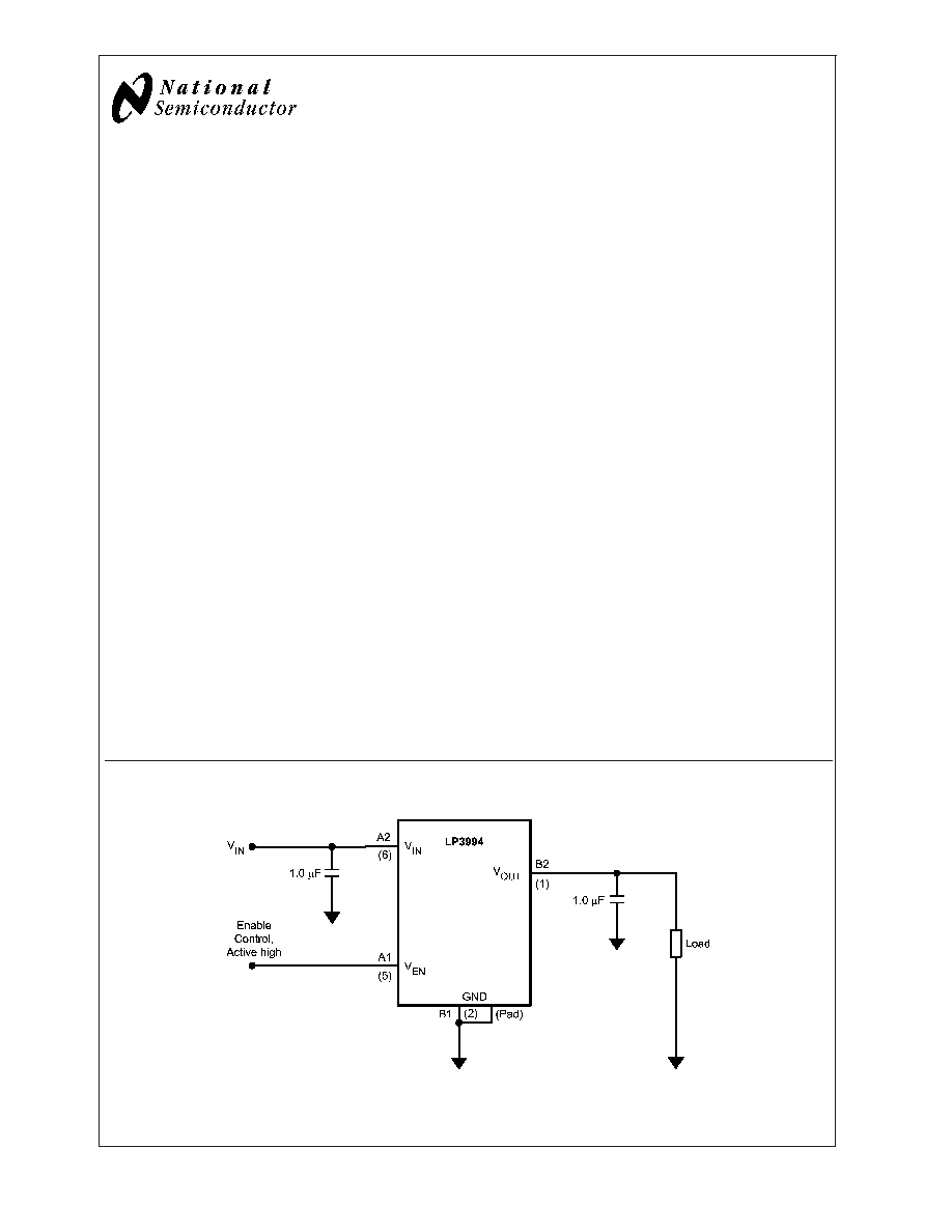
Typical Application Circuit
20046501
August 2004
LP3994
50mA
CMOS
V
oltage
Regulator
with
Enable
Control
© 2004 National Semiconductor Corporation
DS200465
www.national.com
Pin Descriptions
Packages micro SMD-4 and LLP-6
Pin No
micro
SMD
Pin No
LLP
Symbol
Name and Function
A1
5
V
EN
Enable Input; Enables the Regulator when
1.2V
Disables the Regulator when
0.4V
B1
2
GND
Common Ground
B2
1
V
OUT
Voltage output. A 1.0µF Low ESR Capacitor should be connected
to this Pin. Connect this output to the load circuit.
A2
6
V
IN
Voltage Supply Input. A 1.0µF capacitor should be connected at
this input.
3
No Connection. Do not connect to any other device pins.
4
No Connection. Do not connect to any other device pins.
pad
Connect to ground for good thermal operation.
Connection Diagrams
20046502
micro SMD-4 Package
See NS package number TLA04
20046507
LLP- 6 Package (SOT23 footprint)
See NS Package Number LDE06A
LP3994
www.national.com
2
Absolute Maximum Ratings
(Notes 1, 2)
If Military/Aerospace specified devices are required,
please contact the National Semiconductor Sales Office/
Distributors for availability and specifications.
Input Voltage
-0.3 to 6.5V
Output Voltage
-0.3 to (V
IN
+ 0.3V) to
6.5V (max)
Enable Input Voltage
-0.3 to (V
IN
+ 0.3V) to
6.5V (max)
Junction Temperature
150°C
Lead Temp.
microSMD
260°C
LLP
235
o
C
Storage Temperature
-65 to 150°C
Continuous Power
Dissipation(Note 3)
Internally Limited
ESD Rating (Note 4)
Human Body Model
2KV
Machine Model
200V
Operating Conditions
(Notes 1, 2)
Input Voltage
2.5 to 5.5V
Enable Input Voltage
0 to (V
IN
+ 0.3V)
Junction Temperature (T
J
) Range
-40°C to 125°C
Ambient Temperature (T
A
) Range
(Note 5)
-40 to 85
o
C
Thermal Properties
Junction to Ambient Thermal Resistance(Note 6)
JA
microSMD package
220
o
C/W
JA
LLP package
88
o
C/W
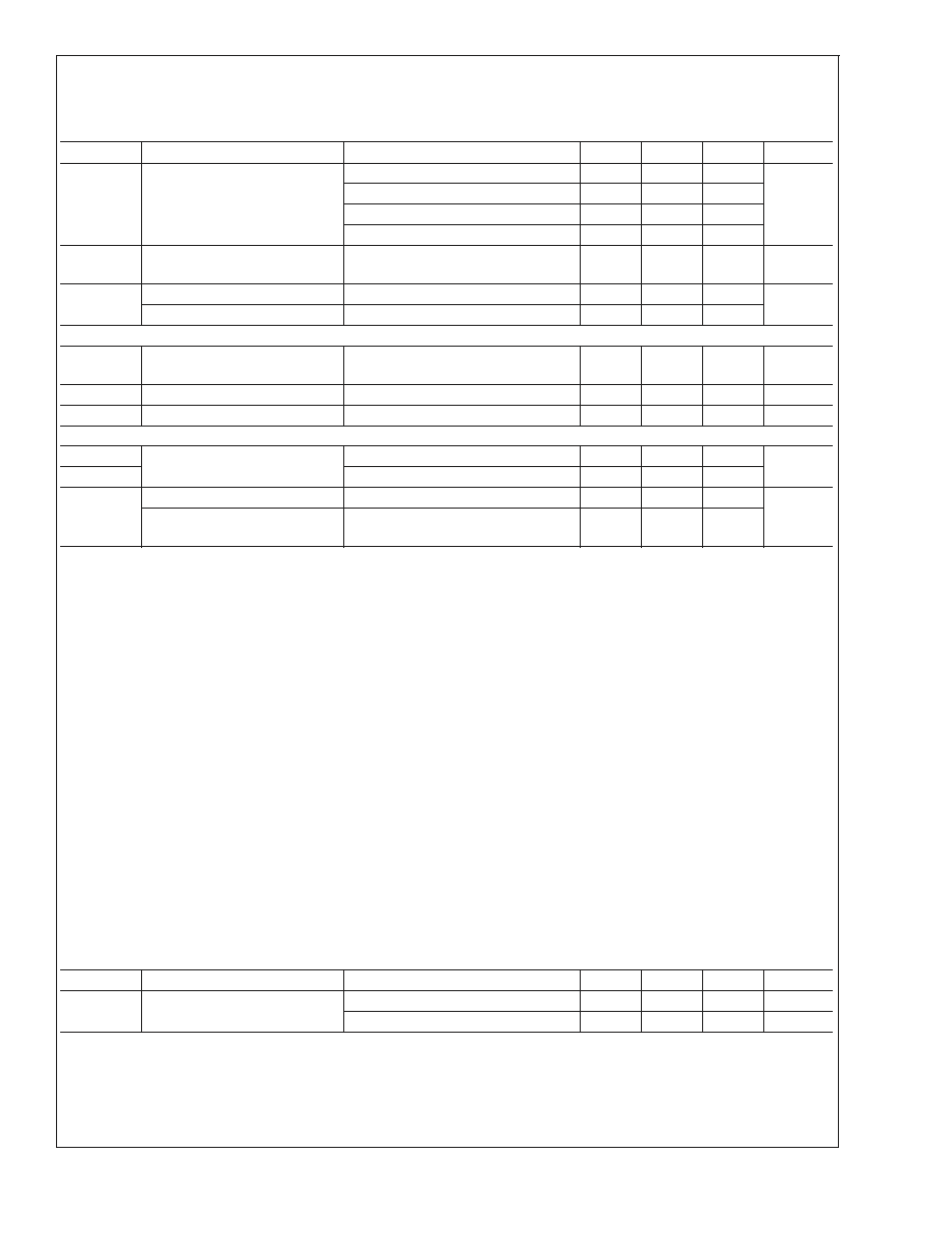
Electrical Characteristics
(Notes 2, 7)
Unless otherwise noted, V
EN
= 1.2, V
IN
= V
OUT
+ 1.0V, C
IN
= 1 µF, I
OUT
= 1 mA, C
OUT
= 1 µF. Typical values and limits ap-
pearing in normal type apply for T
J
= 25°C. Limits appearing in boldface type apply over the full temperature range for opera-
tion, -40 to +125°C. (Notes 13, 14)
Symbol
Parameter
Conditions
Min
Typ
Max
Units
Device Output: V
OUT
1.8V
V
IN
Input Voltage
2.5
5.5
V
V
OUT
Output Voltage Tolerance
Over full line and load regulation.
-60
+60
mV
Line Regulation Error
V
IN
= (V
OUT(NOM)
+ 1.0V) to 5.5V,
I
OUT
= 1mA
0.005
0.07
%/V
Load Regulation Error
I
OUT
= 1mA to 50mA
100
400
µV/mA
I
Q
Quiescent Current
microSMD:
I
OUT
= 0mA
15
35
µA
I
OUT
= 50mA
22
50
LLP:
I
OUT
= 0mA
15
40
I
OUT
= 50mA
25
65
Quiescent Current(Disabled)
V
EN
= 0.4V
0.001
1.5
Device Output: V
OUT
>
1.8V
V
IN
Input Voltage
2.5
5.5
V
V
OUT
Output Voltage Tolerance
Over full line and load regulation.
-90
+90
mV
Line Regulation Error
V
IN
= (V
OUT(NOM)
+ 1.0V) to 5.5V,
I
OUT
= 1mA
0.005
0.1
%/V
Load Regulation Error
I
OUT
= 1mA to 50mA
100
500
µV/mA
Dropout Voltage
(where applicable)
I
OUT
= 1mA
1.5
4.5
mV
I
OUT
= 50mA
75
140
I
Q
Quiescent Current
microSMD:
I
OUT
= 0mA
18
50
µA
I
OUT
= 50mA
22
60
LLP:
I
OUT
= 0mA
20
55
I
OUT
= 50mA
22
65
Quiescent Current(Disabled)
V
EN
= 0.4V
0.001
1.5
Full V
OUT
RANGE
I
LOAD
Load Current
(Notes 8, 9)
0
µA
I
SC
Short Circuit Current Limit
(Note 12)
235
mA
LP3994
www.national.com
4
Electrical Characteristics
(Notes 2, 7) (Continued)
Unless otherwise noted, V
EN
= 1.2, V
IN
= V
OUT
+ 1.0V, C
IN
= 1 µF, I
OUT
= 1 mA, C
OUT
= 1 µF. Typical values and limits ap-
pearing in normal type apply for T
J
= 25°C. Limits appearing in boldface type apply over the full temperature range for opera-
tion, -40 to +125°C. (Notes 13, 14)
Symbol
Parameter
Conditions
Min
Typ
Max
Units
PSRR
Power Supply Rejection Ratio
f = 100Hz, I
OUT
= 1mA to 50mA
70
dB
f = 50kHz, I
OUT
= 1mA to 50mA
30
f = 1MHz, I
OUT
= 1mA
50
f = 1MHz, I
OUT
= 50mA
40
E
n
Output noise Voltage (Note 9)
BW = 100Hz to 100kHz,
V
IN
= 4.2V, I
OUT
= 1mA
95
µV
RMS
T
SHUTDOWN
Thermal Shutdown Temperature
160
°C
Thermal Shutdown Hysteresis
20
Enable Control Characteristics
I
EN
Maximum Input Current at
V
EN
Input
V
EN
= 0.0V and V
IN
= 5.5V
0.015
µA
V
IL
Low Input Threshold
V
IN
= 2.5V to 5.5V
0.4
V
V
IH
High Input Threshold
V
IN
= 2.5V to 5.5V
1.2
V
Timing Characteristics
T
ON1
Turn On Time (Note 9)
10 to 90% of V
OUT(NOM)
(Note 10)
10
20
µS
T
ON2
To 95% Level (Note 11)
35
100
Transient
Response
Line Transient Response |
V
OUT
| Figure 1 (Note 9)
20
mV
Load Transient Response
|
V
OUT
|
Figure 2 (Note 9)
70
Note 1: Absolute Maximum Ratings are limits beyond which damage can occur. Operating Ratings are conditions under which operation of the device is
guaranteed. Operating Ratings do not imply guaranteed performance limits. For guaranteed performance limits and associated test conditions, see the Electrical
Characteristics tables.
Note 2: All Voltages are with respect to the potential at the GND pin.
Note 3: Internal thermal shutdown circuitry protects the device from permanent damage
Note 4: The human body is 100pF discharge through 1.5kW resistor into each pin. The machine model is a 200 pF capacitor discharged directly into each pin.
Note 5: In applications where high power dissipation and/or poor thermal resistance is present, the maximum ambient temperature may have to be derated.
Maximum ambient temperature (T
A(max)
) is dependant on the maximum operating junction temperature (T
J(max-op)
), the maximum power dissipation (P
D(max)
), and
the junction to ambient thermal resistance in the application (
JA
). This relationship is given by :-
T
A(max)
= T
J(max-op)
- (P
D(max)
x
JA
)
See Applications section.
Note 6: Junction to ambient thermal resistance is highly application and board layout dependent. In applications where high maximum power dissipation exists, the
thermal dissipation issues should be addressed in the board layout design.
Note 7: Min and Max limits are guaranteed by design, test, or statistical analysis. Typical numbers are not guaranteed, but do represent the most likely norm.
Note 8: The device maintains the regulated output voltage without the load.
Note 9: This electrical specification is guaranteed by design.
Note 10: Time for V
OUT
to rise from 10 to 90% of V
OUT(nom)
.
Note 11: Time from V
EN
= 1.2V to V
OUT
= 95%(V
OUT(nom)
).
Note 12: Short circuit current is measured on the input supply line at the point when the short circuit condition reduces the output voltage to 95% of its nominal value.
Note 13: C
IN
, and C
OUT
: Low ESR surface mont devices used in setting electrical characteristics.
Note 14: All limits are guaranteed. All electrical characteristics having room-temperature limits are tested during production at T
J
= 25°C or correlated using
Statistical Quality Control methods. Operation over the temperature specification is guaranteed by correlating the electrical characteristics to process and
temperature variations and applying statistical process control.
Output Capacitor, Recommended Specifications
Symbol
Parameter
Conditions
Min
Typ
Max
Units
C
o
Output Capacitor
Capacitance(Note 15)
0.7
1.0
µF
ESR
5
500
m
Note 15: The capacitor tolerance should be
±
30% or better over the full temperature range. The full range of operating conditions for the capacitor in the application
should be considered during device selection to ensure this minimum capacitance specification is met. X7R capacitor types are recommended to meet the full device
temperature range, however X5R, Y5V, and Z5U types may be used with careful consideration of the application and its operating conditions. (See Capacitor
Sections in Application Hints.)
LP3994
www.national.com
5