LP3997
Micropower 250mA CMOS LDO Regulator with Error
Flag / Power-On-Reset
General Description
The LP3997 regulator is designed to meet the requirements
of portable, battery-powered systems, providing accurate
output voltage, low noise, and low quiescent current. The
LP3997 provides 3.3V output at up to 250mA load current.
When switched in shutdown mode, the power consumption
is virtually zero.
The LP3997 is designed to be stable with space saving
ceramic capacitors as small as 1µF.
The LP3997 also includes an out-of-regulation error flag.
When the output is more than 5% below its nominal voltage,
the error flag sets to low. If a capacitor is connected to
device's delay pin, a delayed power-on reset signal will be
generated.
Features
n
Low, 140mV, Dropout at 250mA Load.
n
Stable with Ceramic Capactor.
n
Low Noise, with Bypass Capacitor.
n
Less than 70µA Typical I
Q
at 250mA.
n
Virtually Zero I
Q
(Disabled).
n
Themal and Short Circuit Protection.
n
3.3V Output.
n
For other voltage options, please contact your local NSC
sales office.
Package
8 Lead MSOP
For other package options contact your NSC sales office.
Applications
n
Portable Consumer Electronics
n
Cellular Handsets
n
Laptop and Palm Computers
n
PDA's
n
Digital Cameras
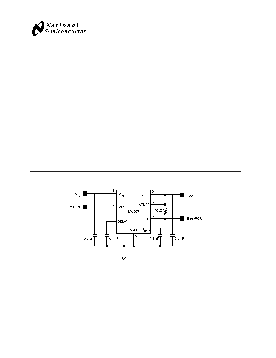
Typical Application Circuit
20092901
PRELIMINARY
May 2004
LP3997
Micropower
250mA
CMOS
LDO
Regulator
with
Error
Flag
/
Power-On-Reset
© 2004 National Semiconductor Corporation
DS200929
www.national.com
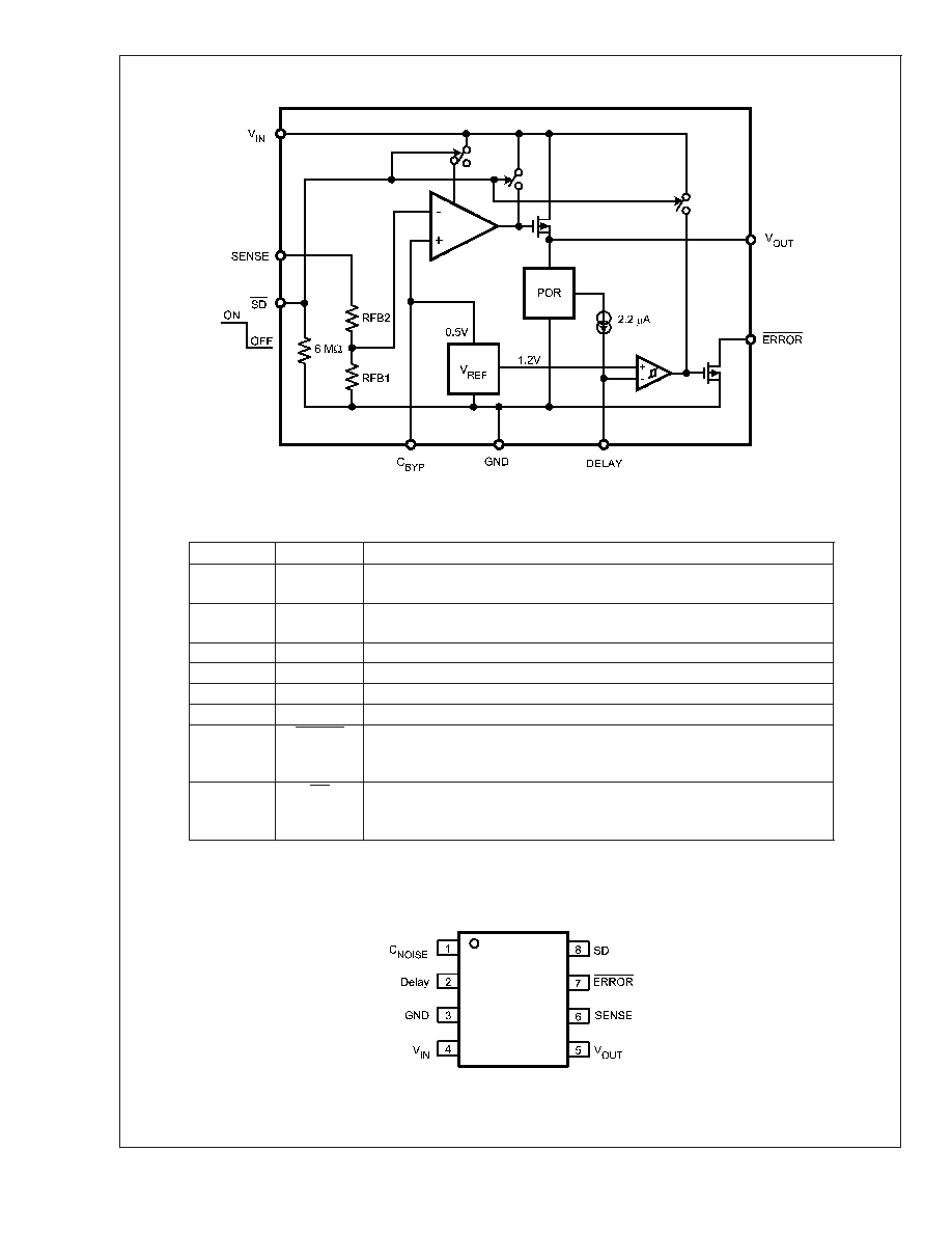
Functional Block Diagram
20092908
Pin Descriptions
Pin #
Name
Description
1
CNOISE
Noise bypass pin. For low noise applications a 0.1µF or larger ceramic
capacitor should be connected from this pin to ground
2
DELAY
A capacitor connected from this pin to ground will allow a delayed
power-on-reset signal at the ERROR (pin 7) output.
3
GND
Ground pin. Local ground for C
NOISE
and C
OUT
.
4
V
IN
Input supply pin. Bypass this with a 1µF capacitor.
5
V
OUT
Output voltage, Connect C
OUT
between this pin and ground.
6
SENSE
Connect this pin to VOUT (pin 5).
7
ERROR
This open drain output is an error flag output which goes low when V
OUT
drops 5% below it nominal voltage. This pin also provides a power-on-reset
signal if a capacitor is connected to the DELAY pin.
8
SD
Shutdown. Disables the regulator when less than 0.4V is applied. Enables the
regulator when greater than 0.9V. The Shutdown pin is pulled down internally
by a 6M
resistor.
Connection Diagram
8 Lead MSOP
NS Package Number MUA08A
20092904
LP3997
www.national.com
2
Ordering Information
For MSOP Package
Please contact Sales Office for Availability
Output
Voltage (V)
Grade
LP3997 Supplied as 1000
Units, Tape and Reel
LP3997 Supplied as 3500
Units, Tape and Reel
Package Marking
3.3
STD
LP3997MM-3.3
LP3997MMX-3.3
LP3997
www.national.com
3
Absolute Maximum Ratings
(Notes 2, 1)
If Military/Aerospace specified devices are required,
please contact the National Semiconductor Sales Office/
Distributors for availability and specifications.
Input Voltage
-0.3 to 6.5V
Output Voltage
-0.3 to (V
IN
+ 0.3V) to
6.5V (max)
SD Input Voltage
-0.3 to (V
IN
+ 0.3V) to
6.5V (max)
Junction Temperature
150∞C
Lead/Pad Temp.
MSOP
260∞C
Storage Temperature
-65 to 150∞C
Continuous Power Dissipation
Internally Limited (Note 3)
ESD (Note 4)
Human Body Model
2KV
Machine Model
200V
Operating Ratings
(Note 1)
Input Voltage
2V to 6V
Shutdown Input Voltage
0 to (V
IN
+ 0.3V) to
6.5V (max)
Junction Temperature
-40∞C to 125∞C
Ambient Temperature T
A
Range
(Note 5)
-40∞C to 85∞C
Thermal Properties
(Note 1)
Junction To Ambient Thermal
Resistance (Note 6)
JA
(MSOP)
210∞C/W
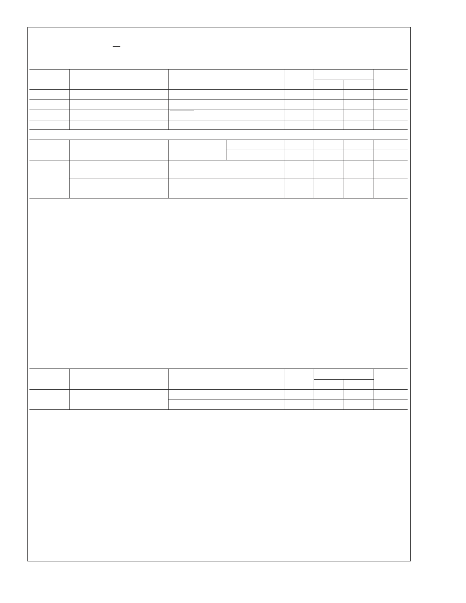
Electrical Characteristics
Unless otherwise noted, V
SD
=950mV, V
IN
= V
OUT
+ 1.0V, C
IN
= 2.2 µF, I
OUT
= 1 mA, C
OUT
=2.2 µF and C
NOISE
= 0.1 µF.
Typical values and limits appearing in normal type apply for T
J
= 27∞C. Limits appearing in boldface type apply over the full
temperature range for operation, -40 to +125∞C. (Note 11)
Symbol
Parameter
Conditions
Typ
Limit
Units
Min
Max
V
IN
Input Voltage
2
6
V
V
OUT
Output Voltage Tolerance
Over full line and load regulation.
-3
+3
%
Line Regulation Error
V
IN
= (V
OUT(NOM)
+ 1.0V) to 6.0V,
I
OUT
= 1mA
0.05
%/V
Load Regulation Error
I
OUT
= 1mA to 250mA
20
µV/mA
I
LOAD
Load Current
(Notes 7, 8)
0
µA
I
Q
Quiescent Current
V
SD
= 950mV, I
OUT
= 0mA
45
µA
V
SD
= 950mV, I
OUT
= 250mA
65
V
SD
= 0.4V
0.002
I
SC
Short Circuit Current Limit
(Note 9)
650
1000
mA
I
OUT
Maximum Output Current
250
mA
PSRR
Power Supply Rejection Ratio
f = 1kHz, I
OUT
= 1mA to 150mA
64
dB
f = 10kHz, I
OUT
= 150mA
39
e
N
Output noise Voltage (Note 8)
BW = 10Hz to
100kHz,
V
IN
= VOUT
nom
+1V
w/o C
NOISE
180
µV
RMS
C
NOISE
= 0.1µF
100
T
SHUTDOWN
Thermal Shutdown
Temperature
160
∞C
Hysteresis
20
Enable Control Characteristics
I
SD
Maximum Input Current at
V
SD
Input
V
SD
= 0.0V
0.001
0.1
µA
V
SD
= 6V (Note 10)
1
2
V
IL
Low Input Threshold
V
IN
= 2V to 6V
0.4
V
V
IH
High Input Threshold
V
IN
= 2V to 6V
0.95
V
Error Flag Characteristics
V
TH
Power Good Trip Threshold
V
IN
Rising
95
95
97
%V
OUT
LP3997
www.national.com
4
Electrical Characteristics
(Continued)
Unless otherwise noted, V
SD
=950mV, V
IN
= V
OUT
+ 1.0V, C
IN
= 2.2 µF, I
OUT
= 1 mA, C
OUT
=2.2 µF and C
NOISE
= 0.1 µF.
Typical values and limits appearing in normal type apply for T
J
= 27∞C. Limits appearing in boldface type apply over the full
temperature range for operation, -40 to +125∞C. (Note 11)
Symbol
Parameter
Conditions
Typ
Limit
Units
Min
Max
V
HYST
Hysteresis
V
IN
Rising or Falling
2
%V
OUT
V
OL
ErrorOutput low Voltage
I
SINK
= 2mA
0.4
V
I
OFF
Error Output High Leakage
ERROR = V
OUT(NOM)
2
µA
I
DELAY
Delay Pin Current Source
V
OUT
>
95% V
OUT(NOM)
2.2
µA
Timing Characteristics
t
ON
Turn On Time (Note 8)
To 95% Level
w/o C
NOISE
150
250
µs
C
NOISE
= 0.1µF
2
ms
Transient
Response
Line Transient Response |
V
OUT
| T
rise
= T
fall
= 30µs (Note 8)
V
IN
= 600mV
8
TBA
mV
(pk - pk)
Load Transient Response
|
V
OUT
|
T
rise
= T
fall
= 1µs (Note 8)
I
OUT
= 1mA to 150mA
70
80
mV
Note 1: Absolute Maximum Ratings are limits beyond which damage can occur. Operating Ratings are conditions under which operation of the device is
guaranteed. Operating Ratings do not imply guaranteed performance limits. For guaranteed performance limits and associated test conditions, see the Electrical
Characteristics tables.
Note 2: All Voltages are with respect to the potential at the GND pin.
Note 3: Internal thermal shutdown circuitry protects the device from permanent damage.
Note 4: The human body model is 100pF discharged through a 1.5k
resistor into each pin. The machine model is a 200pF capacitor discharged directly into each
pin.
Note 5: The maximum ambient temperature (T
A(max)
) is dependant on the maximum operating junction temperature (T
J(max-op)
= 125∞C), the maximum power
dissipation of the device in te application (P
D(max)
), and the junction to ambient thermal resistance of the part/package in the application (
JA
), as given by the
following equation: T
A(max)
= T
J(max-op)
- (
JA
x P
D(max)
).
Note 6: Junction to ambient thermal resistance is dependant on the application and board layout. In applications where high maximum power dissipation is possible,
special care must be paid to thermal dissipation issues in board design.
Note 7: The device maintains the regulated output voltage without the load.
Note 8: This electrical specification is guaranteed by design.
Note 9: Short circuit current is measured on the input supply line at the point when the short circuit condition reduces the output voltage to 5% of its nominal value.
Note 10: Enable Pin has 6M
typical, resistor connected to GND.
Note 11: All limits are guaranteed. All electrical characteristics having room-temperature limits are tested during production at T
J
= 25∞C or correlated using
Statistical Quality Control methods. Operation over the temperature specification is guaranteed by correlating the electrical characteristics to process and
temperature variations and applying statistical process control.
Output Capacitor, Recommended Specifications
Symbol
Parameter
Conditions
Typ
Limit
Units
Min
Max
C
o
Output Capacitor
Capacitance(Note 12)
1.0
0.7
µF
ESR
5
500
m
Note 12: The capacitor tolerance should be 30% or better over temperature. The full operating conditions for the application should be considered when selecting
a suitable capacitor to ensure that the minimum value of capacitance is always met. Recommended capacitor type is X7R. However, dependent on application, X5R,
Y5V, and Z5U can also be used. (See capacitor characteristics section in Application Hints)
LP3997
www.national.com
5