LP5527
Tiny LED Driver for Camera Flash and 4 LEDs with I
2
C
Programmability, Connectivity Test and Audio
Synchronization
General Description
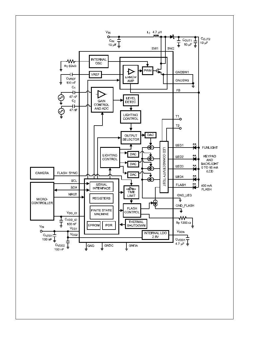
The LP5527 is a lighting management unit for handheld
devices with I
2
C compatible control interface. The LP5527
has a step-up DC/DC converter with high current output and
it drives display and keypad backlights and powers the cam-
era flash LED. In addition the DC/DC converter has the
output current to power for example an audio amplifier si-
multaneously. The chip has four 8-bit programmable high
efficiency constant current LED drivers and a FLASH LED
driver. Built-in audio synchronization feature allows the user
to synchronize one of the LEDs to audio input.
The LP5527 has an integrated 400 mA flash driver with a
safety stop feature and 50 mA torch mode. An external
enable pin is provided for the synchronizing the flash with the
camera action. An external software independent test inter-
face provides a fast way to find a broken path or short on
LED circuits. Very small microSMD package together with
minimum number of external components is a best fit for
handheld devices.
Features
n
High current boost DC-DC converter (up to 1A output
current)
n
Programmable boost output voltage
n
400 mA flash LED constant current driver with low
tolerance and a safety circuit
n
Synchronization pin for the flash timing
n
Two single-ended audio inputs with gain control
n
Four constant current 15 mA LED drivers with 8-bit
programmable brightness control
n
Audio synchronization feature
n
I
2
C compatible control interface
n
Built-in LED connectivity test to maximize manufacturing
yield
n
Small microSMD-30 package (2.5 mm x 3.0 mm x 0.6
mm)
Applications
n
Camera FLASH, funlight and backlight driving in battery
powered devices
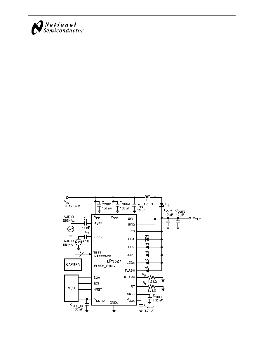
Typical Application
20184001
May 2006
LP5527
T
iny
LED
Driver
for
Camera
Flash
and
4
LEDs
with
I
2
C
Programmability
,
Connectivity
T
est
and
Audio
Synchronization
© 2006 National Semiconductor Corporation
DS201840
www.national.com
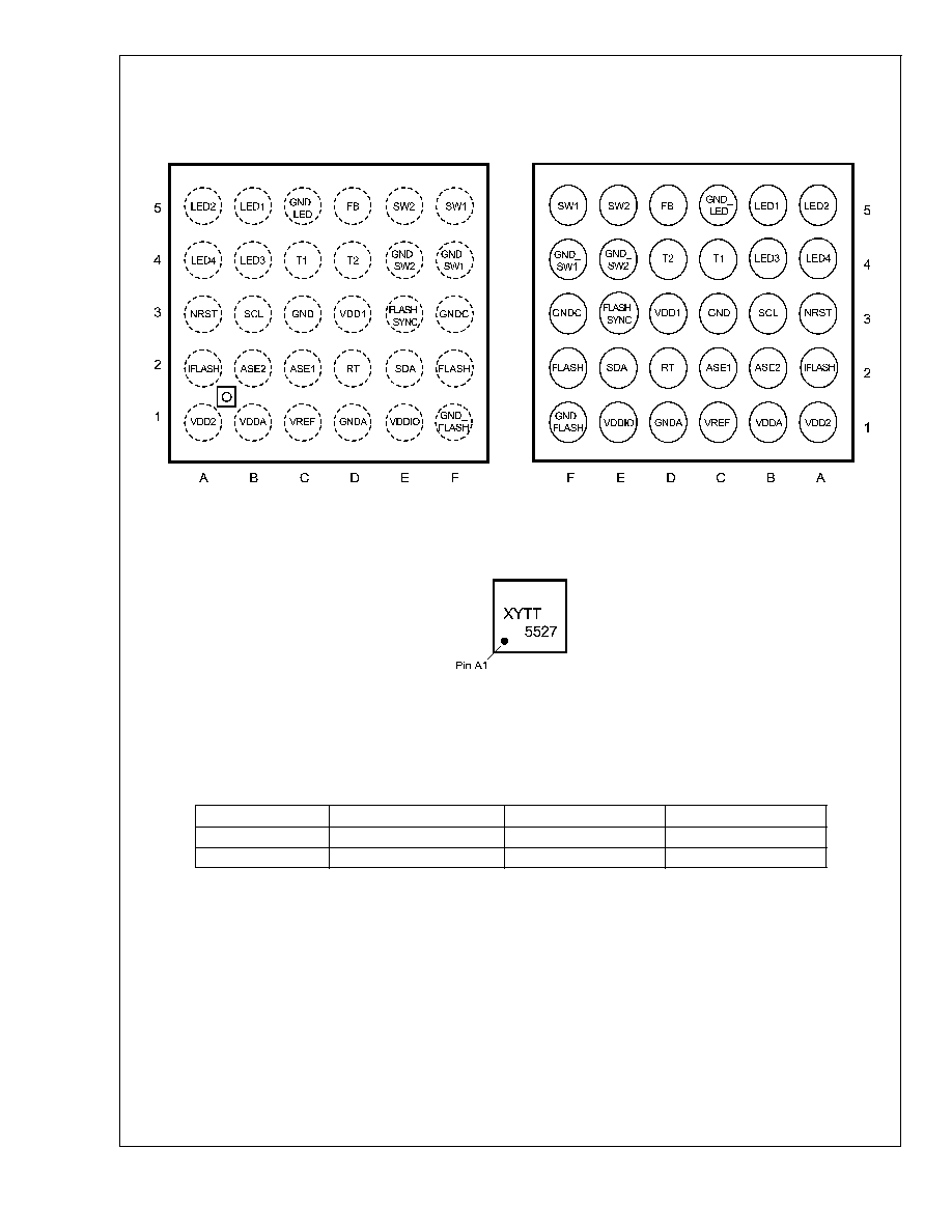
Connection Diagrams and Package Mark Information
microSMD-30 package, 2.466 x
2.974 x 0.60 mm body size, 0.5 mm pitch NS Package Number TLA3011A (Continued)
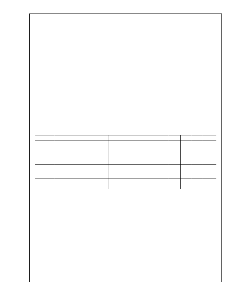
Pin Descriptions
Pin
Name
Type
Description
D3
VDD1
P
Supply Voltage
A1
VDD2
P
Supply Voltage
F5
SW1
A
Boost Converter Switch
E5
SW2
A
Boost Converter Switch
D5
FB
A
Boost Converter Feedback
B5
LED1
O
LED1 Driver Output
A5
LED2
O
LED2 Driver Output
B4
LED3
O
LED3 Driver Output
A4
LED4
O
LED4 Driver Output
F2
FLASH
O
Flash LED Driver Output
F3
GNDC
G
Ground for Core Circuitry
D2
RT
A
Oscillator Frequency Setting
C1
VREF
A
Reference Voltage
B1
VDDA
P
Internal LDO
F4
GND_SW1
G
Boost Converter Ground
E4
GND_SW2
G
Boost Converter Ground
C5
GND_LED
G
LEDs 1 to 4 Driver Ground Connection
F1
GND_FLASH
G
Flash Driver Ground Connection
A2
IFLASH
A
Resistor for Flash Current Setting
D1
GNDA
G
Analog Ground Connection
C3
GND
G
Ground
E1
VDD_IO
P
Supply Voltage for Digital Interface
A3
NRST
DI
Low Active Reset
B3
SCL
DI
I
2
C Compatible Interface Clock Signal
E2
SDA
OD
I
2
C Compatible Interface Data Signal
E3
FLASH_SYNC
DI
FLASH LED Control
D4
T2
DO
Test Pin (Result)
C4
T1
DI
Test Pin (Clock)
C2
ASE1
AI
Audio Input
B2
ASE2
AI
Audio Input
A: Analog Pin D: Digital Pin G: Ground Pin P: Power Pin
I: Input Pin I/O: Input/Output Pin O: Output Pin OD: Open Drain Pin
LP5527
www.national.com
3
Absolute Maximum Ratings
(Notes 1, 2)
If Military/Aerospace specified devices are required,
please contact the National Semiconductor Sales Office/
Distributors for availability and specifications.
Voltage on power pins (V
DD1,2
)
-0.3V to +6.0V
Voltage on analog pins
-0.3V to V
DD1,2
+0.3V
with 6.0V max
Voltage on input/output pins
-0.3V to V
DD1,2
+0.3V
with 6.0V max
V(all other pins): Voltage to GND
-0.3V to 6.0V
I(V
REF
)
10 µA
I(FLASH)
500 mA
Continuous Power Dissipation
(Note 3)
Internally Limited
Junction Temperature (T
J-MAX
)
125
o
C
Storage Temperature Range
-65
o
C to +150
o
C
Maximum Lead Temperature
(Reflow soldering, 3 times)
(Note 4)
260
o
C
ESD Rating (Note 5)
Human Body Model
2 kV
Operating Ratings
(Note 1)
,
(Note 2)
Voltage on power pins (V
DD1,2
)
3.0 to 5.5V
Voltage on ASE1, ASE2
0V to 1.6V
V
DD_IO
1.65V to V
DD1
Junction Temperature (T
J
) Range
-30
o
C to +125
o
C
Ambient Temperature (T
A
) Range
(Note 6)
-30
o
C to +85
o
C
Thermal Properties
Junction-to-Ambient Thermal
Resistance (
JA
),
TLA3011A Package (Note 7)
60 - 100
o
C/W
Electrical Characteristics
(Notes 2, 8)
Limits in standard typeface are for T
J
= 25
o
C. Limits in boldface type apply over the operating ambient temperature range
(-30
o
C
<
T
A
<
+85
o
C). Unless otherwise noted, specifications apply to the LP5527 Block Diagram with: V
IN
= 3.6V, C
IN
=
10 µF, C
OUT1
= 10 µF, C
OUT2
= 10 µF, C
VDD_IO
= 100 nF, C
VREF
= 100 nF, C
VDDA
= 4.7 µF, C
VDD1
= 100 nF, C
VDD2
= 100
nF, L
1
= 4.7 µH. (Note 9)
Symbol
Parameter
Condition
Min
Typ
Max
Units
I
SHUT DOWN
Current of V
DD1
+ V
DD2
pins +
Leakage Current of SW1, SW2,
LED1 to 4 and FLASH
Voltage on V
DD_IO
= 0V, NRST = L,
NSTBY(bit) = L
1
5
µA
I
DD
Active Mode Supply Current
(V
DD1
+ V
DD2
current)
NRST = H, NSTBY(bit) = H, no load,
EN_BOOST(bit) = L, SCL, SDA = H
350
µA
I
DD
No load supply current
(V
DD1
+ V
DD2
current)
NSTBY(bit) = H, EN_BOOST(bit) = H,
SCL, SDA, NRST = H,
AUTOLOAD_EN(bit) = L
850
µA
I
VDDIO
V
DD_IO
Standby Supply current
NSTBY(bit) = L
1
µA
V
DDA
I
VDDA
= 1 mA
-4%
2,8V
+4%
V
Note 1: Absolute Maximum Ratings indicate limits beyond which damage to the component may occur. Operating Ratings are conditions under which operation of
the device is guaranteed. Operating Ratings do not imply guaranteed performance limits. For guaranteed performance limits and associated test conditions, see the
Electrical Characteristics tables.
Note 2: All voltages are with respect to the potential at the GND pins.
Note 3: Internal thermal shutdown circuitry protects the device from permanent damage. Thermal shutdown engages at T
J
=160
o
C (typ.) and disengages at
T
J
=140
o
C (typ.).
Note 4: For detailed soldering specifications and information, please refer to National Semiconductor Application Note AN1112 : Micro SMD Wafer Level Chip Scale
Package.
Note 5: The Human body model is a 100 pF capacitor discharged through a 1.5 k
resistor into each pin. MIL-STD-883 3015.7
Note 6: In applications where high power dissipation and/or poor package thermal resistance is present, the maximum ambient temperature may have to be
derated. Maximum ambient temperature (T
A-MAX
) is dependent on the maximum operating junction temperature (T
J-MAX-OP
= 125
o
C), the maximum power
dissipation of the device in the application (P
D-MAX
), and the junction-to ambient thermal resistance of the part/package in the application (
JA
), as given by the
following equation: T
A-MAX
= T
J-MAX-OP
≠ (
JA
x P
D-MAX
).
Note 7: Junction-to-ambient thermal resistance is highly application and board-layout dependent. In applications where high maximum power dissipation exists,
special care must be paid to thermal dissipation issues in board design.
Note 8: Min and Max limits are guaranteed by design, test, or statistical analysis. Typical numbers are not guaranteed, but do represent the most likely norm.
Note 9: Low-ESR Surface-Mount Ceramic Capacitors (MLCCs) used in setting electrical characteristics.
LP5527
www.national.com
4