LP5900
Ultra Low Noise, 100 mA Linear Regulator for RF/Analog
Circuits Requires No Bypass Capacitor
General Description
The LP5900 is a linear regulator capable of supplying 100
mA output current. Designed to meet the requirements of
RF/Analog circuits, the LP5900 device provides low noise,
high PSRR, low quiescent current, and low line transient
response figures. Using new innovative design techniques
the LP5900 offers class-leading device noise performance
without a noise bypass capacitor.
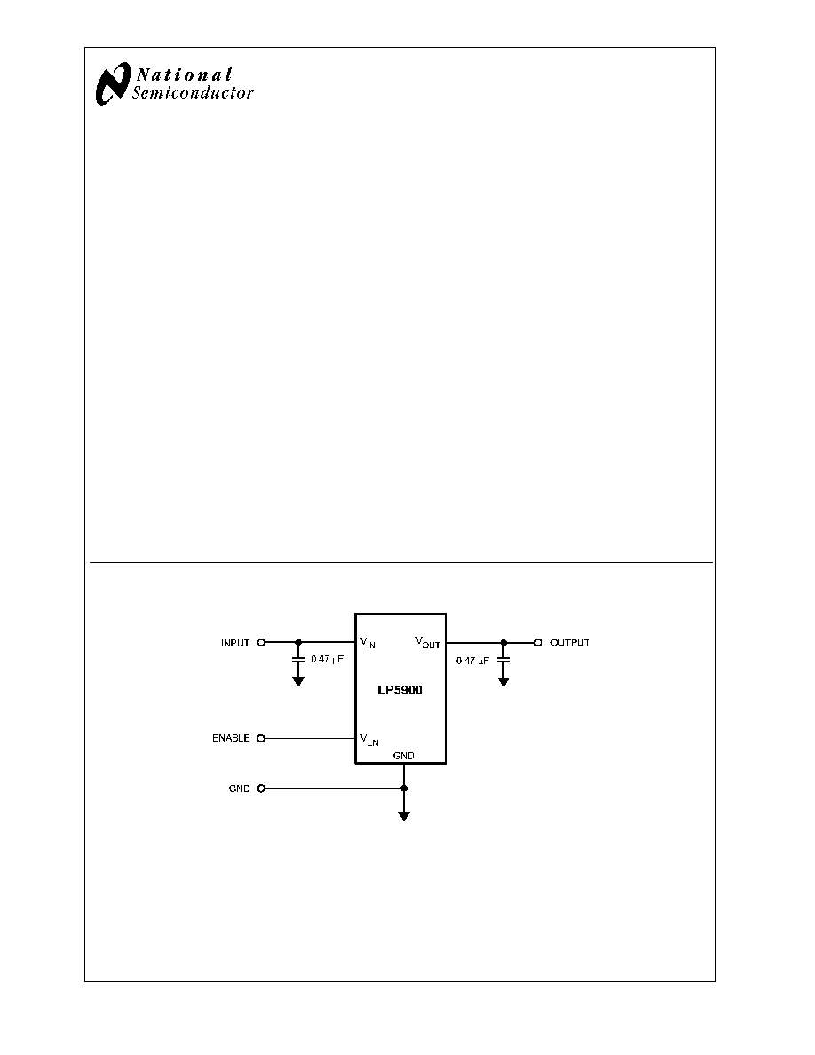
The device is designed to work with 0.47 µF input and output
ceramic capacitors. (No Bypass Capacitor is required)
This device is available with 1.5V, 1.8V, 2.0V, 2.2V, 2.5V,
2.8V, 3.0V, and 3.3V outputs. Please contact your local sales
office for any other voltage options.
Features
n
Stable with 0.47 µF Ceramic Input and Output
Capacitors
n
No Noise Bypass Capacitor Required
n
Logic Controlled Enable
n
Thermal-overload and short-circuit protection
n
-40∞C to +125∞C junction temperature range for
operation
Key Specifications
n
Input voltage range
2.5V to 5.5V
n
Output voltage range
1.5V to 3.3V
n
Output current
100 mA
n
Low output voltage noise
6.5 µV
RMS
n
PSRR
85 dB at 1 kHz
n
Output voltage tolerance
±
2%
n
Virtually zero I
Q
(disabled)
<
1 µA
n
Very low I
Q
(enabled)
25 µA
n
Start-up time
150 µs
n
Low dropout
80 mV typ.
Package
4-Bump micro SMD
(lead free)
1.057 mm x 1.083 mm
Applications
n
Cellular phones
n
PDA handsets
n
Wireless LAN devices
Typical Application Circuit
20144101
July 2005
LP5900
Ultra
Low
Noise,
100
mA
Linear
Regulator
for
RF/Analog
Circuits
Requires
No
Bypass
Capacitor
© 2005 National Semiconductor Corporation
DS201441
www.national.com
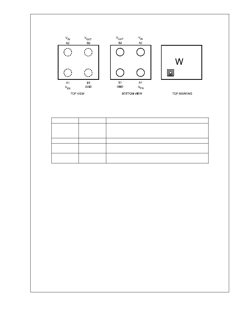
Connection Diagrams
4-Bump Thin micro SMD Package, Large Bump
NS Package Number TLA04
20144102
The actual physical placement of the package marking will vary from part to part.
Pin Descriptions
Pin #
Symbol
Name and Function
A1
V
EN
Enable input; disables the regulator when
0.4V. Enables the
regulator when
1.2V. An internal 1 M pulldown resistor
connects this input to ground.
B1
GND
Common ground
B2
V
OUT
Output voltage. A 0.47 µF Low ESR capacitor should be connected
to this Pin. Connect this output to the load circuit.
A2
V
IN
Input voltage supply. A 0.47 µF capacitor should be connected at
this input.
LP5900
www.national.com
2
Absolute Maximum Ratings
(Notes 1, 2)
If Military/Aerospace specified devices are required,
please contact the National Semiconductor Sales Office/
Distributors for availability and specifications.
V
IN
Pin: Input Voltage
-0.3 to 6.0V
V
OUT
Pin: Output Voltage
-0.3 to (V
IN
+ 0.3V) to
6.0V (max)
V
EN
Pin: Enable Input Voltage
-0.3 to (V
IN
+ 0.3V) to
6.0V (max)
Continuous Power Dissipation
(Note 3)
Internally Limited
Junction Temperature (T
JMAX
)
150∞C
Storage Temperature Range
-65 to 150∞C
Maximum Lead Temperature
(Soldering, 10 sec.)
265∞C
ESD Rating (Note 4)
Human Body Model
2 kV
Machine Model
200V
Operating Ratings
(Note 1)
,
(Note 2)
V
IN
: Input Voltage Range
2.5V to 5.5V
V
EN
: Enable Voltage Range
0 to (V
IN
+ 0.3V) to
5.5V (max)
Recommended Load Current
(Note 5)
0 to 100 mA
Junction Temperature Range (T
J
)
-40∞C to +125∞C
Ambient Temperature Range (T
A
)
(Note 5)
-40∞C to +85∞C
Thermal Properties
Junction to Ambient Thermal Resistance
JA
(Note 6)
JEDEC Board (Note 16)
88∞C/W
4L Cellphone Board
157.4∞C/W
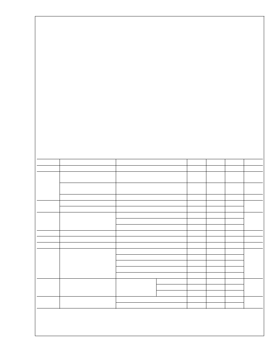
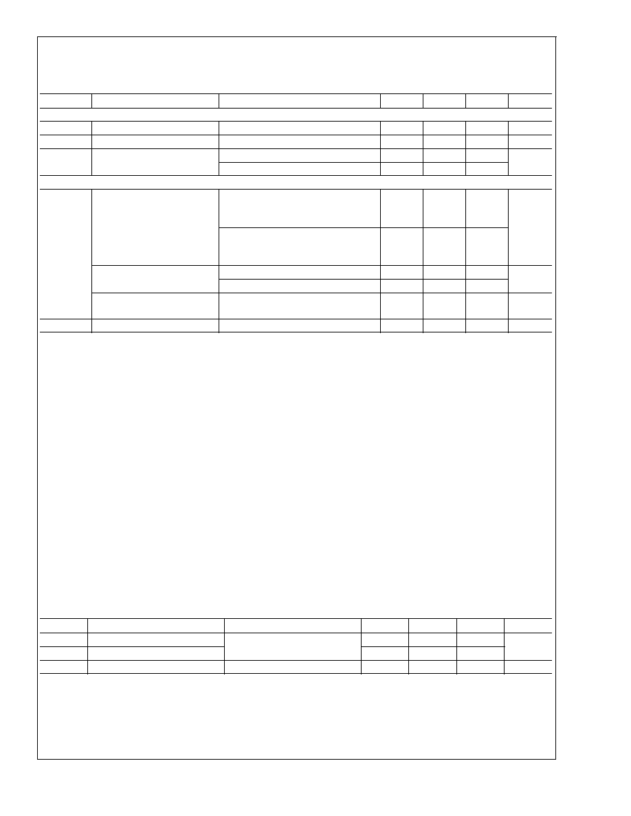
Electrical Characteristics
Limits in standard typeface are for T
A
= 25
o
C. Limits in boldface type apply over the full operating junction temperature range
(-40
o
C
T
J
+125
o
C). Unless otherwise noted, specifications apply to the LP5900 Typical Application Circuit (pg. 1) with: V
IN
= V
OUT (NOM)
+ 1.0V, V
EN
= 1.2V, C
IN
= C
OUT
= 0.47 µF, I
OUT
= 1.0 mA. (Note 2), (Note 7)
Symbol
Parameter
Conditions
Min
Typ
Max
Units
V
IN
Input Voltage
2.5
5.5
V
V
OUT
Output Voltage Tolerance
V
IN
= (V
OUT(NOM)
+ 1.0V) to 5.5V, I
OUT
= 1 mA to 100mA
-2
2
%
Line Regulation
V
IN
= (V
OUT(NOM)
+ 1.0V) to 5.5V, I
OUT
= 1 mA
0.05
%/V
Load Regulation
I
OUT
= 1 mA to 100 mA
0.001
%/mA
I
LOAD
Load Current
(Note 9)
0
mA
Maximum Output Current
(Note 15)
100
I
Q
Quiescent Current (Note 11)
V
EN
= 1.2V, I
OUT
= 0 mA
25
50
µA
V
EN
= 1.2V, I
OUT
= 100 mA
100
200
V
EN
= 0.3V (Disabled)
0.003
1.0
I
G
Ground Current (Note 13)
I
OUT
= 0 mA (V
OUT
= 2.5V)
30
µA
V
DO
Dropout Voltage
I
OUT
= 100 mA
80
150
mV
I
SC
Short Circuit Current Limit
(Note 12)
300
mA
PSRR
Power Supply Rejection Ratio
(Note 15)
f = 100 Hz, I
OUT
= 100 mA
85
dB
f = 1 kHz, I
OUT
= 100 mA
75
f = 10 kHz, I
OUT
= 100 mA
65
f = 50 kHz, I
OUT
= 100 mA
52
f = 100 kHz, I
OUT
= 100 mA
40
e
n
Output Noise Voltage
(Note 15)
BW = 10 Hz to 100
kHz, V
IN
= 4.2V
I
OUT
= 0 mA
7
µV
RMS
I
OUT
= 1 mA
10
I
OUT
= 100 mA
6.5
T
SHUTDOWN
Thermal Shutdown
Temperature
160
o
C
Hysteresis
20
LP5900
www.national.com
4
Electrical Characteristics
(Continued)
Limits in standard typeface are for T
A
= 25
o
C. Limits in boldface type apply over the full operating junction temperature range
(-40
o
C
T
J
+125
o
C). Unless otherwise noted, specifications apply to the LP5900 Typical Application Circuit (pg. 1) with: V
IN
= V
OUT (NOM)
+ 1.0V, V
EN
= 1.2V, C
IN
= C
OUT
= 0.47 µF, I
OUT
= 1.0 mA. (Note 2), (Note 7)
Symbol
Parameter
Conditions
Min
Typ
Max
Units
Login Input Thresholds
V
IL
Low Input Threshold (V
EN
)
V
IN
= 2.5V to 5.5V
0.4
V
V
IH
High Input Threshold (V
EN
)
V
IN
= 2.5V to 5.5V
1.2
V
I
EN
Input Current at V
EN
Pin
(Note 14)
V
EN
= 5.5V and V
IN
= 5.5V
5.5
µA
V
EN
= 0.0V and V
IN
= 5.5V
0.001
Transient Characteristics
V
OUT
Line Transient
(Note 15)
V
IN
= (V
OUT(NOM
) + 1.0V) to
(V
OUT(NOM
) + 1.6V) in 30 µs, I
OUT
= 1
mA
-2
mV
V
IN
= (V
OUT(NOM)
+ 1.6V) to
(V
OUT(NOM)
+ 1.0V) in 30 µs, I
OUT
= 1
mA
2
Load Transient
(Note 15)
I
OUT
= 1 mA to 100 mA in 10 µs
-70
mV
I
OUT
= 100 mA to 1 mA in 10 µs
30
Overshoot on Startup
(Note 15)
20
mV
Turn on Time
To 95% of V
OUT(NOM)
150
300
µs
Note 1: Absolute Maximum Ratings indicate limits beyond which damage to the component may occur. Operating Ratings are conditions under which operation of
the device is guaranteed. Operating Ratings do not imply guaranteed performance limits. For guaranteed performance limits and associated test conditions, see the
Electrical Characteristics tables.
Note 2: All voltages are with respect to the potential at the GND pin.
Note 3: Internal thermal shutdown circuitry protects the device from permanent damage.
Note 4: The Human body model is a 100 pF capacitor discharged through a 1.5 k
resistor into each pin. The machine model is a 200 pF capacitor discharged
directly into each pin. MIL-STD-883 3015.7
Note 5: In applications where high power dissipation and/or poor package thermal resistance is present, the maximum ambient temperature may have to be
derated. Maximum ambient temperature (T
A-MAX
) is dependent on the maximum operating junction temperature (T
J-MAX-OP
= 125∞C), the maximum power
dissipation of the device in the application (P
D-MAX
), and the junction-to ambient thermal resistance of the part/package in the application (
JA
), as given by the
following equation: T
A-MAX
= T
J-MAX-OP
≠ (
JA
x P
D-MAX
). See applications section.
Note 6: Junction-to-ambient thermal resistance is highly application and board-layout dependent. In applications where high maximum power dissipation exists,
special care must be paid to thermal dissipation issues in board design.
Note 7: Min and Max limits are guaranteed by design, test, or statistical analysis. Typical numbers are not guaranteed, but do represent the most likely norm.
Note 8: C
IN
, C
OUT
: Low-ESR Surface-Mount Ceramic Capacitors (MLCCs) used in setting electrical characteristics.
Note 9: The device maintains a stable, regulated output voltage without a load current.
Note 10: Dropout voltage is the voltage difference between the input and the output at which the output voltage drops to 100 mV below its nominal value. This
parameter only applies to output voltages above 2.5V.
Note 11: Quiescent current is defined here as the difference in current between the input voltage source and the load at V
OUT
.
Note 12: Short Circuit Current is measured with V
OUT
pulled to 0v and V
IN
worst case = 6.0V.
Note 13: Ground current is defined here as the total current flowing to ground as a result of all input voltages applied to the device.
Note 14: There is a 1 M
resistor between V
EN
and ground on the device.
Note 15: This specification is guaranteed by design.
Note 16: Detailed description of the board can be found in JESD51-7
Output & Input Capacitor, Recommended Specifications
Symbol
Parameter
Conditions
Min
Nom
Max
Units
C
IN
Input Capacitance
Capacitance for stability
0.33
0.47
µF
C
OUT
Output Capacitance
0.33
0.47
10
ESR
Output/Input Capacitance
5
500
m
Note: The minimum capacitance should be greater than 0.33 µF over the full range of operating conditions. The capacitor tolerance should be 30% or better over
the full temperature range. The full range of operating conditions for the capacitor in the application should be considered during device selection to ensure this
minimum capacitance specification is met. X7R capacitors are recommended however capacitor types X5R, Y5V and Z5U may be used with consideration of the
application and conditions.
LP5900
www.national.com
5