LP5951
Micropower, 150mA Low-Dropout CMOS Voltage
Regulator
General Description
The LP5951 regulator is designed to meet the requirements
of portable, battery-powered systems providing a regulated
output voltage and low quiescent current. When switched to
shutdown mode via a logic signal at the Enable pin, the
power consumption is reduced to virtually zero.
The LP5951 is designed to be stable with small 1ĶF/1.5ĶF
ceramic capacitors.
The LP5951 also features internal protection against short-
circuit currents and over-temperature conditions.
Performance is specified for a -40įC to 125įC temperature
range.
The device is available in SOT23-5 and SC70-5 package.
The device is available in fixed output voltages in the range
of 1.3V to 3.3V. For availability, please contact your local
NSC sales office.
Features
n
Excellent line transient response:
Ī
2mV typ.
n
Excellent PSRR: -60dB at 1kHz typ.
n
Low quiescent current of 29ĶA typ.
n
1.8 to 5.5V input voltage range
n
Small SC70-5 and SOT23-5 packages
n
Fast turn-on time of 30Ķs typ.
n
Typ.
<
1nA quiescent current in shutdown
n
Guaranteed 150mA output current
n
Output voltage range: 1.3V to 3.3V
n
Logic controlled enable 0.4V/0.9V
n
Good load transient response of 50mVpp typ.
n
Thermal-overload and short-circuit protection
n
-40įC to +125įC junction temperature range
Applications
n
General purpose
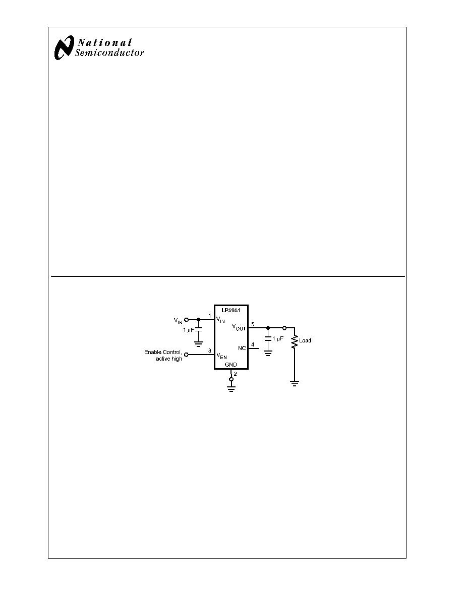
Typical Application Circuit
20136201
August 2006
LP5951
Micropower
,
150mA
Low-Dropout
CMOS
V
oltage
Regulator
© 2006 National Semiconductor Corporation
DS201362
www.national.com
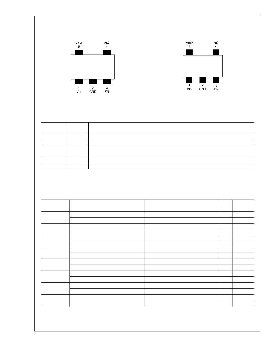
Connection Diagrams
5-Lead Small Outline Package
SOT23-5 (MF)
5-Lead Small Outline Package
SC70-5 (MG)
20136202
Top View
See NS Package Number MF05A
20136203
Top View
See NS Package Number MAA05A
Pin Descriptions
Pin
Number
Pin Name
Description
1
V
IN
Input Voltage. Input range: 1.8V to 5.5V
2
GND
Ground
3
EN
Enable pin logic input: Low = shutdown, High = normal operation. This pin should not be left
floating.
4
NC
No internal connection
5
V
OUT
Regulated output voltage
Order Information
For 5-Lead Small Outline Package SOT23-5 (MF)
Output
Voltage (V)
LP5951 Supplied as 1000 Units,
Tape and Reel
LP5951 Supplied as 3000 Units,
Tape and Reel
Flow
Package
Marking
1.3
LP5951MF-1.3
LP5951MFX-1.3
LKRB
LP5951MF-1.3
LP5951MFX-1.3
NOPB
LKRB
1.5
LP5951MF-1.5
LP5951MFX-1.5
LKAB
LP5951MF-1.5
LP5951MFX-1.5
NOPB
LKAB
1.8
LP5951MF-1.8
LP5951MFX-1.8
LKBB
LP5951MF-1.8
LP5951MFX-1.8
NOPB
LKBB
2.0
LP5951MF-2.0
LP5951MFX-2.0
LKCB
LP5951MF-2.0
LP5951MFX-2.0
NOPB
LKCB
2.5
LP5951MF-2.5
LP5951MFX-2.5
LKEB
LP5951MF-2.5
LP5951MFX-2.5
NOPB
LKEB
2.8
LP5951MF-2.8
LP5951MFX-2.8
LKFB
LP5951MF-2.8
LP5951MFX-2.8
NOPB
LKFB
3.0
LP5951MF-3.0
LP5951MFX-3.0
LKGB
LP5951MF-3.0
LP5951MFX-3.0
NOPB
LKGB
3.3
LP5951MF-3.3
LP5951MFX-3.3
LKHB
LP5951MF-3.3
LP5951MFX-3.3
NOPB
LKHB
LP5951
www.national.com
2
Order Information
(Continued)
For 5-Lead Small Outline Package SC70-5 (MG)
Output
Voltage (V)
LP5951 Supplied as 1000 Units,
Tape and Reel
LP5951 Supplied as 3000 Units,
Tape and Reel
Flow
Package
Marking
1.3
LP5951MG-1.3
LP5951MGX-1.3
L23
LP5951MG-1.3
LP5951MGX-1.3
NOPB
L23
1.5
LP5951MG-1.5
LP5951MGX-1.5
L2B
LP5951MG-1.5
LP5951MGX-1.5
NOPB
L2B
1.8*
LP5951MG-1.8
LP5951MGX-1.8
L3B
LP5951MG-1.8
LP5951MGX-1.8
NOPB
L3B
2.0*
LP5951MG-2.0
LP5951MGX-2.0
L4B
LP5951MG-2.0
LP5951MGX-2.0
NOPB
L4B
2.5*
LP5951MG-2.5
LP5951MGX-2.5
L5B
LP5951MG-2.5
LP5951MGX-2.5
NOPB
L5B
2.8*
LP5951MG-2.8
LP5951MGX-2.8
L6B
LP5951MG-2.8
LP5951MGX-2.8
NOPB
L6B
3.0*
LP5951MG-3.0
LP5951MGX-3.0
L7B
LP5951MG-3.0
LP5951MGX-3.0
NOPB
L7B
3.3*
LP5951MG-3.3
LP5951MGX-3.3
LAB
LP5951MG-3.3
LP5951MGX-3.3
NOPB
LAB
* Not yet released. For availability please contact your local NSC sales office.
Note: The package marking on the backside of the component designates the date code and a NSC internal code for die traceability. It will vary considerably.
SOT23-5: ZWTT
SC70-5: WTT
with:
Z: 1 Digit Assembly Plant Code,
W: 1 Digit Date Code,
TT: 2 Digit Dierun Code
LP5951
www.national.com
3
Absolute Maximum Ratings
(Notes 2,
1)
If Military/Aerospace specified devices are required,
please contact the National Semiconductor Sales Office/
Distributors for availability and specifications.
V
IN
pin: Voltage to GND
-0.3V to 6.5V
EN pin: Voltage to GND
-0.3V to (V
IN
+0.3V)
with 6.5V max
Continuous Power
Dissipation(Note 3)
Internally Limited
Junction Temperature (T
J-MAX
)
150įC
Storage Temperature Range
-65įC to + 150įC
Package Peak Reflow
Temperature (10-20 sec.)
240įC
Package Peak Reflow
Temperature (Pb-free, 10-20 sec.)
260įC
ESD Rating(Note 4)
Human Body Model:
2.0kV
Machine Model
200V
Operating Ratings
(Notes 1, 2)
Input Voltage Range (V
IN
)
1.8V to 5.5V
V
EN
Input Voltage
0 to (V
IN
+ 0.3V)
Junction Temperature (T
J
) Range
-40įC to + 125įC
Ambient Temperature (T
A
) Range
(Note 5)
Thermal Properties
Junction-to-Ambient Thermal
Resistance (
JA
), (Note 6)
SOT23-5 Package:
220įC/W
SC70-5 Package:
415įC/W
ESD Caution Notice
National Semiconductor recommends that all integrated circuits be handled with appropriate precautions. Failure to observe
proper ESD handling techniques can result in damage.
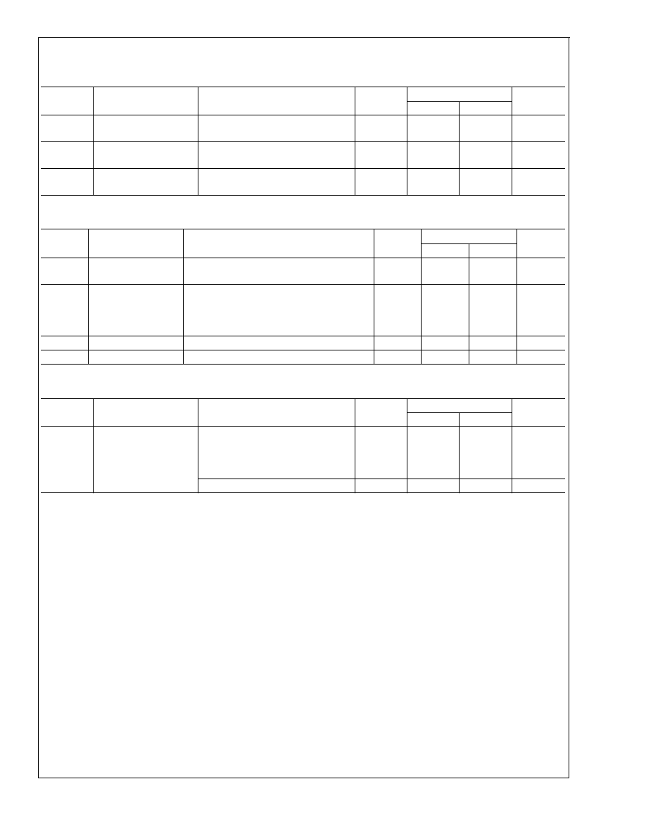
Electrical Characteristics
(Notes 2, 7)
Typical values and limits appearing in standard typeface are for T
A
= 25įC. Limits appearing in boldface type apply over the
full operating temperature range: -40įC
T
J
+125įC. Unless otherwise noted, V
IN
= V
OUT(NOM)
+ 1V, C
IN
= 1ĶF, C
OUT
= 1ĶF,
V
EN
= 0.9V.
Symbol
Parameter
Condition
Typ
Limit
Units
Min
Max
V
IN
Input Voltage
V
IN
V
OUT(NOM)
+ V
DO
1.8
5.5
V
V
OUT
Output Voltage
Tolerance
I
OUT
= 1mA
-30įC
T
J
+125įC
-2.0
-3.5
2.0
3.5
%
%
Line Regulation Error
V
IN
= V
OUT(NOM)
+ 1V to 5.5V
I
OUT
= 1mA
0.1
%/V
Load Regulation Error
I
OUT
= 1mA to 150mA
-0.01
%/mA
V
DO
Output Voltage Dropout
(Note 10)
I
OUT
= 150mA
V
OUT
2.5V
V
OUT
<
2.5V
200
250
350
mV
mV
I
Q
Quiescent Current
V
EN
= 0.9V, I
LOAD
= 0
V
EN
= 0.9V, I
LOAD
= 150mA
V
EN
= 0V
29
33
0.005
55
70
1
ĶA
ĶA
ĶA
I
SC
Output Current
(short circuit)
V
IN
= V
OUT(NOM)
+ 1V
400
150
mA
PSRR
Power Supply
Rejection Ratio
Sine modulated V
IN
f = 100Hz
f = 1kHz
f = 10kHz
60
60
50
dB
dB
dB
E
N
Output Noise
BW = 10Hz - 100kHz
125
ĶV
RMS
TSD
Thermal Shutdown
160
įC
Temperature Hysteresis
20
įC
LP5951
www.national.com
4
Electrical Characteristics
(Notes 2, 7)
(Continued)
Enable Control Characteristics
Symbol
Parameter
Conditions
Typical
Limit
Units
Min
Max
I
EN
Maximum Input Current
at V
EN
Input
0V
V
EN
V
IN
, V
IN
= 5.5V
-1
1
ĶA
V
IL
Low Input Threshold
(shutdown)
V
IN
= 1.8..5.5V
0.4
V
V
IH
High Input Threshold
(enable)
V
IN
= 1.8..5.5V
0.9
V
Transient Characteristics
Symbol
Parameter
Conditions
Typical
Limit
Units
Min
Max
V
OUT
Dynamic Line
Transient
V
IN
= V
OUT(NOM)
+ 1V to
V
OUT(NOM)
+ 1V + 0.6V in 30Ķs, no load
Ī
2
mV
V
OUT
Dynamic Load
Transient
I
OUT
= 0mA to 150mA in 10Ķs
I
OUT
= 150mA to 0mA in 10Ķs
I
OUT
= 1mA to 150mA in 1Ķs
I
OUT
= 150mA to 1mA in 1Ķs
-30
20
-50
40
mV
mV
mV
mV
V
OUT
Overshoot on Startup
Nominal conditions
10
mV
T
ON
Turn on time
I
OUT
= 1mA
30
Ķs
Output Capacitor, Recommended Specification
Symbol
Parameter
Conditions
Value
Limit(Note 8)
Units
Min
Max
C
OUT
Output Capacitance
Capacitance (Note 9)
I
OUT
= 150mA, V
IN
= 5.0V
V
OUT
<
2.8V
V
OUT
2.8V
1.0
1.5
0.7
1.1
47
47
ĶF
ĶF
ESR
0.003
0.300
Note 1: Absolute Maximum Ratings indicate limits beyond which damage to the component may occur. Operating Ratings are conditions under which operation of
the device is guaranteed. Operating Ratings do not imply guaranteed performance limits. For guaranteed performance limits and associated test conditions, see the
Electrical Characteristics tables.
Note 2: All voltages are with respect to the potential at the GND pin.
Note 3: Internal thermal shutdown circuitry protects the device from permanent damage. Thermal shutdown engages at T
J
= 160įC (typ.) and disengages at T
J
=
140įC (typ.).
Note 4: The Human body model is a 100pF capacitor discharged through a 1.5k
resistor into each pin. The machine model is a 200pF capacitor discharged
directly into each pin. (MIL-STD-883 3015.7)
Note 5: In applications where high power dissipation and/or poor package thermal resistance is present, the maximum ambient temperature may have to be
derated. Maximum ambient temperature (T
A-MAX
) is dependent on the maximum operating junction temperature (T
J-MAX-OP
= 125įC), the maximum power
dissipation of the device in the application (P
D-MAX
), and the junction-to ambient thermal resistance of the part/package in the application (
JA
), as given by the
following equation: T
A-MAX
= T
J-MAX-OP
≠ (
JA
x
PD-MAX
).
Note 6: Junction-to-ambient thermal resistance is highly application and board-layout dependent. In applications where high maximum power dissipation exists,
special attention must be paid to thermal dissipation issues in board design.
Note 7: Min and Max limits are guaranteed by design, test, or statistical analysis. Typical numbers are not guaranteed, but do represent the most likely norm.
Note 8: Min and Max limits are guaranteed by design
Note 9: The capacitor tolerance should be 30% or better over temperature. The full operating conditions for the application should be considered when selecting
a suitable capacitor to ensure that the minimum value of capacitance is always met. Recommended capacitor type is X7R. However, dependent on application, X5R,
Y5V, and Z5U can also be used. The shown minimum limit represents real minimum capacitance, including all tolerances and must be maintained over temperature
and dc bias voltage (See capacitor section in Applications Hints)
Note 10: Dropout voltage is defined as the input to output voltage differential at which the output voltage falls to 100mV below the nominal output voltage. This
specification does not apply for output voltages below 1.8V.
LP5951
www.national.com
5