 | –≠–ª–µ–∫—Ç—Ä–æ–Ω–Ω—ã–π –∫–æ–º–ø–æ–Ω–µ–Ω—Ç: LPV7215MG | –°–∫–∞—á–∞—Ç—å:  PDF PDF  ZIP ZIP |
LPV7215
580 nA Rail-to-Rail Input and Output, 1.8V, Push-Pull
Output Comparator
General Description
The LPV7215 is an ultra low-power comparator with a typical
power supply current of 580 nA. It has the best-in-class
power supply current versus propagation delay performance
available among National's low-power comparators. The
propagation delay is as low as 4.5 microseconds with 100
mV overdrive at 1.8V supply.
Designed to operate over a wide range of supply voltages,
from 1.8V to 5.5V, the LPV7215, with guaranteed operation
at 1.8V, 2.7V and 5.0V, is ideal for use in a variety of
battery-powered applications. With rail-to-rail common mode
voltage range, the LPV7215 is well suited for single-supply
operation.
Featuring a push-pull output stage, the LPV7215 allows for
operation with absolute minimum power consumption when
driving any capacitive or resistive load.
With an operating temperature range of -40∞C to 125∞C, this
comparator can be adopted for extreme temperature appli-
cations. Available in a choice of space-saving packages, the
LPV7215 is ideal for use in handheld electronics and mobile
phone applications. The LPV7215 is manufactured with Na-
tional's advanced VIP50 process.
Features
(Typical unless otherwise noted)
n
Ultra low power consumption
580 nA
n
Wide supply voltage range
1.8V to 5.5V
n
Propagation delay
4.5 µs
n
Push-Pull output current drive
19 mA
n
Temperature range
-40∞C to 125∞C
n
Rail-to-rail input
n
Tiny SOT23-5 and SC70-5 packages
Applications
n
Laptop computers
n
Mobile phones
n
RC timers
n
Alarm and monitoring circuits
n
Window comparators
n
Multivibrators
Typical Application
20123601
Threshold Detector
20123602
Propagation Delay vs. Overdrive
PRELIMINARY
September 2005
LPV7215
580
nA
Rail-to-Rail
Input
and
Output,
1.8V
Push-Pull
Output
Comparator
© 2005 National Semiconductor Corporation
DS201236
www.national.com
Absolute Maximum Ratings
(Note 1)
If Military/Aerospace specified devices are required,
please contact the National Semiconductor Sales Office/
Distributors for availability and specifications.
ESD Tolerance (Note 2)
Human Body
2000V
Machine Model
200V
V
IN
Differential
±
2.5V
Supply Voltage (V
+
- V
-
)
6V
Voltage at Input/Output pins
V
+
+0.3V, V
-
-0.3V
Storage Temperature Range
-65∞C to +150∞C
Junction Temperature (Note 3)
+150∞C
Soldering Information
Infrared or Convection (20 sec)
235∞C
Wave Soldering Lead Temp. (10
sec)
260∞C
Operating Ratings
(Note 1)
Temperature Range (Note 3)
-40∞C to +125∞C
Supply Voltage (V
+
≠ V
-
)
1.8V to 5.5V
Package Thermal Resistance (
JA
(Note 3))
5-Pin SOT23
234∞C/W
5-Pin SC70
456∞C/W
1.8V Electrical Characteristics
(Note 8)
Unless otherwise specified, all limits are guaranteed for T
J
= 25∞C, V
+
= 1.8V, V
-
= 0V, and V
CM
= V
+
/2, V
O
= V
-
. Boldface
limits apply at the temperature extremes.
Symbol
Parameter
Conditions
Min
(Note 5)
Typ
(Note 4)
Max
(Note 5)
Units
I
S
Supply Current
V
CM
= 0.3V, T
A
= 25∞C
580
645
nA
V
CM
= 0.3V, -40∞C to 85∞C
681
V
CM
= 0.3V, -40∞C to 125∞C
980
V
CM
= 1.5V, T
A
= 25∞C
790
875
V
CM
= 1.5V, -40∞C to 85∞C
912
V
CM
= 1.5V, -40∞C to 125∞C
1155
V
OS
Input Offset Voltage
V
CM
= 0V
V
CM
= 1.8V
±
0.3
±
3
±
4
mV
TC V
OS
Input Offset Average Drift
(Note 7)
±
2
µV/C
I
B
Input Bias Current (Note 6)
V
CM
= 0.5V
-5
fA
V
CM
= 1.3V
I
OS
Input Offset Current
1
fA
CMRR
Common Mode Rejection
Ratio
V
CM
Stepped from 0V to 0.7V
V
CM
Stepped from 1.2V to 1.8V
80
90
dB
PSRR
Power Supply Rejection Ratio
V
+
= 1.8V to 5V, V
CM
= 0V
75
93
dB
CMVR
Input Common-Mode Voltage
Range
CMRR
50 dB
1.8
0
V
A
V
Voltage Gain
120
dB
V
O
Output Swing High
I
O
= 500 µA
1.68
V
I
O
= 1 mA
1.54
Output Swing Low
I
O
= -500 µA
120
mV
I
O
= -1 mA
260
I
OUT
Output Current
Source
2.0
2.26
mA
Sink
2.7
3.1
Propagation Delay
(High to Low)
Overdrive = 10 mV
Overdrive = 100 mV
13
4.5
µs
Propagation Delay
(Low to High)
Overdrive = 10 mV
Overdrive = 100 mV
12.5
6.6
µs
t
rise
Rise Time
Overdrive = 10 mV
C
L
= 30 pF, R
L
= 1 M
80
ns
Overdrive = 100 mV
C
L
= 30 pF, R
L
= 1 M
80
LPV7215
www.national.com
2
1.8V Electrical Characteristics
(Note 8)
(Continued)
Unless otherwise specified, all limits are guaranteed for T
J
= 25∞C, V
+
= 1.8V, V
-
= 0V, and V
CM
= V
+
/2, V
O
= V
-
. Boldface
limits apply at the temperature extremes.
Symbol
Parameter
Conditions
Min
(Note 5)
Typ
(Note 4)
Max
(Note 5)
Units
t
fall
Fall Time
Overdrive = 10 mV
C
L
= 30 pF, R
L
= 1 M
70
ns
Overdrive = 100 mV
C
L
= 30 pF, R
L
= 1 M
70
2.7V Electrical Characteristics
(Note 8)
Unless otherwise specified, all limits are guaranteed for T
J
= 25∞C, V
+
= 2.7V, V
-
= 0V, and V
CM
= V
+
/2, V
O
= V
-
. Boldface
limits apply at the temperature extremes.
Symbol
Parameter
Conditions
Min
(Note 5)
Typ
(Note 4)
Max
(Note 5)
Units
I
S
Supply Current
V
CM
= 0.3V, T
A
= 25∞C
605
670
nA
V
CM
= 0.3V, -40∞C to 85∞C
707
V
CM
= 0.3V, -40∞C to 125∞C
1005
V
CM
= 2.4V, T
A
= 25∞C
815
905
V
CM
= 2.4V, -40∞C to 85∞C
940
V
CM
= 2.4V, -40∞C to 125∞C
1220
V
OS
Input Offset Voltage
V
CM
= 0V
±
0.3
±
3
±
4
mV
V
CM
= 2.7V
TC V
OS
Input Offset Average Drift
(Note 7)
±
1
µV/C
I
B
Input Bias Current (Note 6)
V
CM
= 0.5V
-5
fA
V
CM
= 2.2V
I
OS
Input Offset Current
1
fA
CMRR
Common Mode Rejection
Ratio
V
CM
Stepped from 0V to 1.6V
80
90
dB
V
CM
Stepped from 2.1V to 2.7V
PSRR
Power Supply Rejection Ratio
V
+
= 1.8V to 5V, V
CM
= 0V
75
93
dB
CMVR
Input Common-Mode Voltage
Range
CMRR
50 dB
2.7
0
V
A
V
Voltage Gain
120
dB
V
O
Output Swing High
I
O
= 500 µA
2.62
V
I
O
= 1 mA
2.54
Output Swing Low
I
O
= -500 µA
80
mV
I
O
= -1 mA
160
I
OUT
Output Current
Source
5.3
5.7
mA
Sink
6
7.5
Propagation Delay
(High to Low)
Overdrive = 10 mV
14.5
µs
Overdrive = 100 mV
6
Propagation Delay
(Low to High)
Overdrive = 10 mV
15
Overdrive = 100 mV
8
t
rise
Rise time
Overdrive = 10 mV
C
L
= 30 pF, R
L
= 1 M
90
ns
Overdrive = 100 mV
C
L
= 30 pF, R
L
= 1 M
85
t
fall
Fall time
Overdrive = 10 mV
C
L
= 30 pF, R
L
= 1 M
85
ns
Overdrive = 100 mV
C
L
= 30 pF, R
L
= 1 M
75
LPV7215
www.national.com
3
5V Electrical Characteristics
(Note 8)
Unless otherwise specified, all limits are guaranteed for T
J
= 25∞C, V
+
= 5V, V
-
= 0V, and V
CM
= V
+
/2, V
O
= V
-
.Boldface limits
apply at the temperature extremes.
Symbol
Parameter
Conditions
Min
(Note 5)
Typ
(Note 4)
Max
(Note 5)
Units
I
S
Supply Current
V
CM
= 0.3V, T
A
= 25∞C
612
677
nA
V
CM
= 0.3V, -40∞C to 85∞C
740
V
CM
= 0.3V, -40∞C to 125∞C
1240
V
CM
= 4.7V, T
A
= 25∞C
825
920
V
CM
= 4.7V, -40∞C to 85∞C
970
V
CM
= 4.7V, -40∞C to 125∞C
1450
V
OS
Input Offset Voltage
V
CM
= 0V
±
0.3
±
3
±
4
mV
V
CM
= 5V
TC V
OS
Input Offset Average Drift
(Note 7)
±
1
µV/C
I
B
Input Bias Current (Note 6)
V
CM
= 0.5V
-5
fA
V
CM
= 4.5V
I
OS
Input Offset Current
1
fA
CMRR
Common Mode Rejection
Ratio
V
CM
Stepped from 0V to 3.9V
80
90
dB
V
CM
Stepped from 4.4V to 5V
PSRR
Power Supply Rejection Ratio
V
+
= 1.8V to 5V, V
CM
= 0V
75
93
dB
CMVR
Input Common-Mode Voltage
Range
CMRR
50 dB
5
0
V
V
O
Output Swing High
I
O
= 500 µA
4.95
V
I
O
= 1 mA
4.9
Output Swing Low
I
O
= -500 µA
50
mV
I
O
= -1 mA
100
I
OUT
Output Current
Source
15.5
17
mA
Sink
16.7
19
Propagation Delay
(High to Low)
Overdrive = 10 mV
Overdrive = 100 mV
18
8
µs
Propagation Delay
(Low to High)
Overdrive = 10 mV
Overdrive = 100 mV
30
13
µs
t
rise
Rise Time
Overdrive = 10 mV
C
L
= 30 pF, R
L
= 1 M
100
ns
Overdrive = 100 mV
C
L
= 30 pF, R
L
= 1 M
100
t
fall
Fall Time
Overdrive = 10 mV
C
L
= 30 pF, R
L
= 1 M
115
ns
Overdrive = 100 mV
C
L
= 30 pF, R
L
= 1 M
95
Note 1: Absolute Maximum Ratings indicate limits beyond which damage to the device may occur. Operating Ratings indicate conditions for which the device is
intended to be functional, but specific performance is not guaranteed. For guaranteed specifications and the test conditions, see the Electrical Characteristics Tables.
Note 2: Human body model, 1.5 k
in series with 100 pF. Machine model: 0 in series with 200 pF.
Note 3: The maximum power dissipation is a function of T
J(MAX)
,
JA
, and T
A
. The maximum allowable power dissipation at any ambient temperature is
P
D
= (T
J(MAX)
- T
A
)/
JA
. All numbers apply for packages soldered directly onto a PC board at the time of characterization.
Note 4: Typical values represent the most likely parametric norm.
Note 5: Limits are 100% production tested at 25∞C. Limits over the operating temperature range are guaranteed through correlations using statistical quality control
(SQC) method.
Note 6: Positive current corresponds to current flowing into the device.
Note 7: Offset voltage average drift determined by dividing the change in V
OS
at temperature extremes into the total temperature change.
Note 8: Electrical table values apply only for factory testing conditions at the temperature indicated. Factory testing conditions result in very limited self-heating of
the device.
LPV7215
www.national.com
4
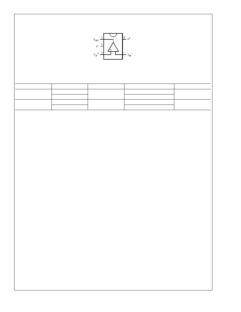
Connection Diagram
SC70/SOT23
20123698
Top View
Ordering Information
Package
Part Number
Package Marking
Transport Media
NSC Drawing
5-Pin SOT-23
LPV7215MF
C30A
1k Units Tape and Reel
MF05A
LPV7215MFX
3k Units Tape and Reel
5-Pin SC70
LPV7215MG
C37
1k Units Tape and Reel
MAA05A
LPV7215MGX
3k Units Tape and Reel
LPV7215
www.national.com
5