 | –≠–ª–µ–∫—Ç—Ä–æ–Ω–Ω—ã–π –∫–æ–º–ø–æ–Ω–µ–Ω—Ç: LQB08A | –°–∫–∞—á–∞—Ç—å:  PDF PDF  ZIP ZIP |
LM4570
Single-Ended Input Motor Driver
General Description
The LM4570 is a single supply motor driver for improved
sensory experience in mobile phones and other handheld
devices. The LM4570 is capable of driving up to 192mA
while operating from a 3V supply. Near rail-to-rail output
swing under load ensures sufficient voltage drive for most
DC motors, while the differential output drive allows the
voltage polarity across the motor to be reversed quickly.
Reversing the voltage gives the LM4570 the ability to drive a
motor both clock-wise and counter clock-wise from a single
supply.
The LM4570 features fast turn on time, and a wide input
voltage range for precise speed control. A low power shut-
down mode minimizes power consumption.
Thermal and output short circuit protection prevents the
device from being damaged during fault conditions.
Key Specifications
j
High Output Current
@
V
DD
= 3V
192mA
j
Fast Turn On Time
@
3V
2.4ms
j
Quiescent Power Supply Current
@
3V
1.9mA
j
Shutdown Current
0.1µA (typ)
Features
n
Output Short Circuit Protection
n
High Output Current Capability
n
Wide Output Voltage Range
n
Fast Turn on Time
n
Output Short Circuit Protection
n
Low Power Shutdown Mode
n
Minimum external components
n
Available in space-saving LLP package
Applications
n
Mobile Phones
n
PDAs
n
Video Game Systems
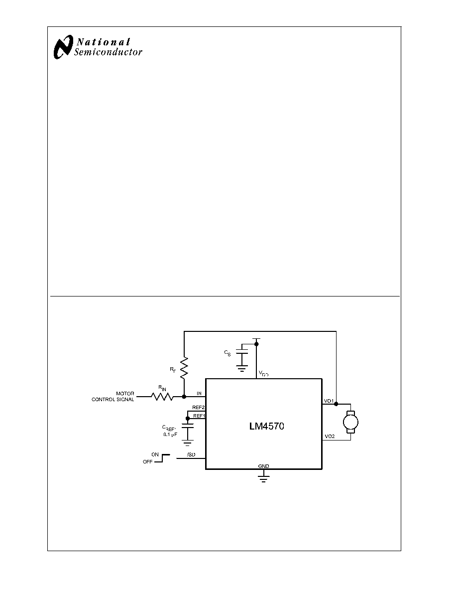
Typical Application
20186326
FIGURE 1. Typical Motor Driver Application Circuit
April 2006
LM4570
Single-Ended
Input
Motor
Driver
© 2006 National Semiconductor Corporation
DS201863
www.national.com
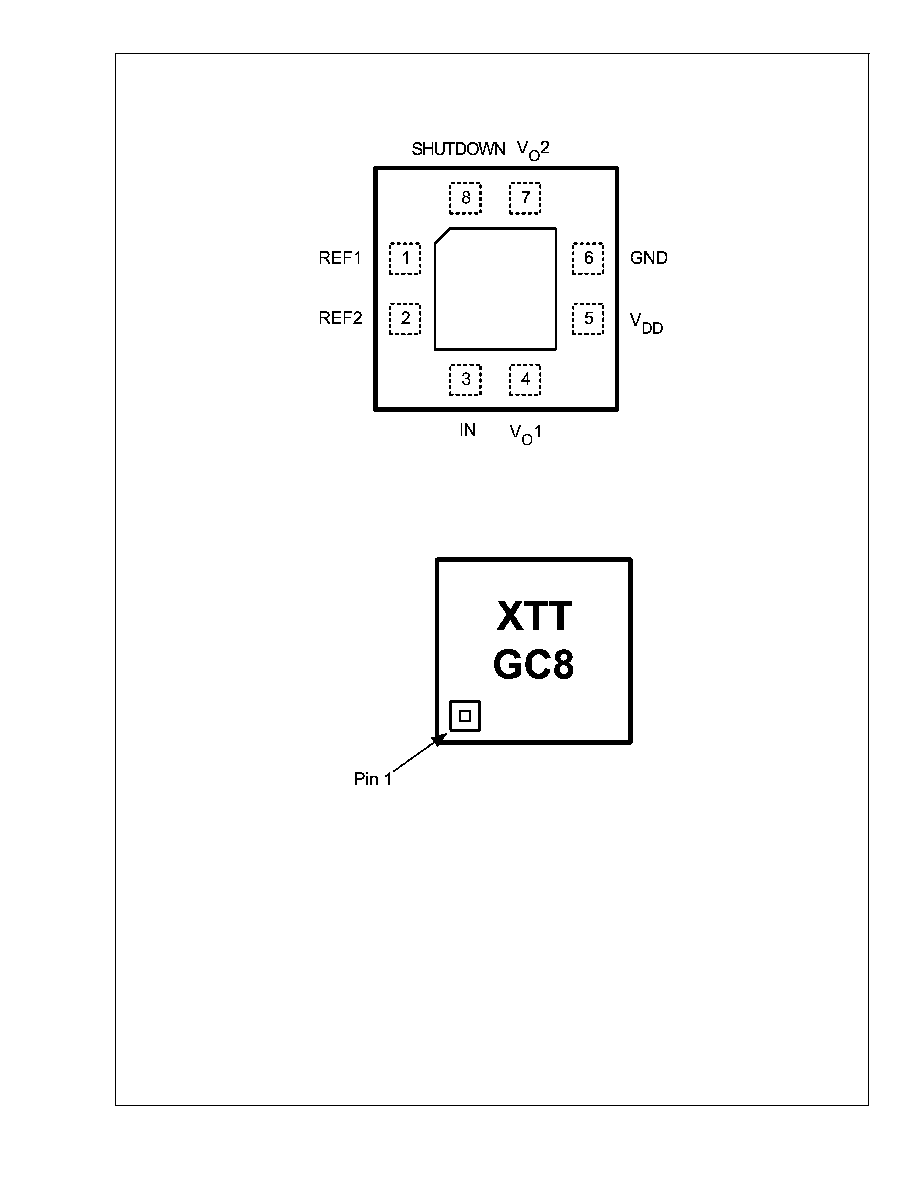
Connection Diagrams
Leadless Leadframe Package (LLP)
LQ Package
20186325
Top View
Order Number LM4570LQ
See NS Package Number LQB08A
LLP Marking
20186327
Top View
X - One digit date code
TT - Lot traceability
G - Boomer Family
C8 - LM4570LQ
LM4570
www.national.com
2
Absolute Maximum Ratings
(Note 2)
If Military/Aerospace specified devices are required,
please contact the National Semiconductor Sales Office/
Distributors for availability and specifications.
Supply Voltage (Note 1)
6.0V
Storage Temperature
-65∞C to +150∞C
Voltage at Any Input Pin
-0.3V
to V
DD
+0.3V
Power Dissipation (Note 3)
Internally Limited
ESD Susceptibility (Note 4)
2000V
ESD Susceptibility (Note 5)
200V
Junction Temperature (T
JMAX
)
150∞C
Thermal Resistance
JA
(LLP)
140∞C/W
Operating Ratings
Temperature Range
T
MIN
T
A
T
MAX
-40∞C
T
A
85∞C
Supply Voltage
2.4V
V
DD
5.5V
Electrical Characteristics V
DD
= 5V
(Notes 1, 2)
The following specifications apply for V
DD
= 5V, A
V-BTL
= 6dB unless otherwise specified. Limits apply for T
A
= 25∞C.
Symbol
Parameter
Conditions
LM4570
Units
(Limits)
Typical
Limit
(Note 6)
(Notes 7, 8)
I
DD
Quiescent Power Supply Current
V
IN
= 0V, I
L
= 0A, No Load
2.5
5.5
mA (max)
V
IN
= 0V, I
L
= 0A, R
L
= 30
2.6
5.5
I
SD
Shutdown Current
V
SD
= GND
0.1
1.5
µA (max)
V
IH
Logic Input High
1.4
V (min)
V
IL
Logic Input Low
0.4
V (max)
V
OS
Output Offset Voltage
5
±
35
mV (max)
I
OUT
Output Current
V
OH
, V
OL
250mV
268
mA
T
WU
Wake-up time
2.5
ms (max)
V
OH
Output High Voltage
R
L
= 30
specified as
|V
DD
- V
OH
|
146
200
mV (max)
V
OL
Output Low Voltage
R
L
= 30
specified as
|GND + V
OH
|
106
200
mV (max)
Electrical Characteristics V
DD
= 3V
(Notes 1, 2)
The following specifications apply for V
DD
= 3V, A
V-BTL
= 6dB unless otherwise specified. Limits apply for T
A
= 25∞C.
Symbol
Parameter
Conditions
LM4570
Units
(Limits)
Typical
Limit
(Note 6)
(Notes 7, 8)
I
DD
Quiescent Power Supply Current
V
IN
= 0V, I
L
= 0A, No Load
1.9
4
mA (max)
V
IN
= 0V, I
L
= 0A, R
L
= 30
1.95
4
I
SD
Shutdown Current
V
SD
= GND
0.1
1.0
µA (max)
V
IH
Logic Input High
1.4
V (min)
V
IL
Logic Input Low
0.4
V (max)
V
OS
Output Offset Voltage
5
±
35
mV (max)
I
OUT
Output Current
V
OH
, V
OL
200mV
192
mA
T
WU
Wake-up time
2.4
ms (max)
V
OH
Output High Voltage
R
L
= 30
specified as
|V
DD
- V
OH
|
90
110
mV (max)
V
OL
Output Low Voltage
R
L
= 30
specified as
|V
DD
- V
OH
|
63
110
mV (max)
LM4570
www.national.com
3

Note 1: All voltages are measured with respect to the ground pin, unless otherwise specified.
Note 2: Absolute Maximum Ratings indicate limits beyond which damage to the device may occur. Operating Ratings indicate conditions for which the device is
functional, but do not guarantee specific performance limits. Electrical Characteristics state DC and AC electrical specifications under particular test conditions which
guarantee specific performance limits. This assumes that the device is within the Operating Ratings. Specifications are not guaranteed for parameters where no limit
is given; however, the typical value is a good indication of device performance.
Note 3: The maximum power dissipation must be de-rated at elevated temperatures and is dictated by T
JMAX
,
JC
, and the ambient temperature T
A
. The maximum
allowable power dissipation is P
DMAX
= (T
JMAX
≠T
A
)/
JA
or the number given in the Absolute Maximum Ratings, whichever is lower. For the LM4570, T
JMAX
= 150∞C
and the typical
JA
for the LLP package is 140∞C/W.
Note 4: Human body model, 100pF discharged through a 1.5k
resistor.
Note 5: Machine Model, 220pF≠240pF discharged through all pins.
Note 6: Typicals are measured at 25∞C and represent the parametric norm.
Note 7: Limits are guaranteed to National's AOQL (Average Outgoing Quality Level).
Note 8: Datasheet min/max specification limits are guaranteed by design, test, or statistical analysis.
Note 9: Shutdown current is measured in a normal room environment. Exposure to direct sunlight will increase I
SD
by a maximum of 2µA.
LM4570
www.national.com
4
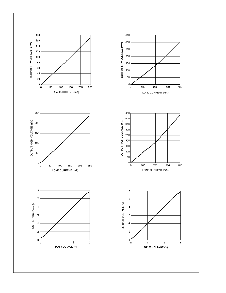
Typical Performance Characteristics
Output Low Voltage vs Load Current
V
DD
= 3V
Output Low Voltage vs Load Current
V
DD
= 5V
20186313
20186312
Output High Voltage vs Load Current
V
DD
= 3V
Output High Voltage vs Load Current
V
DD
= 5V
20186311
20186310
Output Voltage vs Input Voltage
V
DD
= 3V, R
L
= 20
Output Voltage vs Input Voltage
V
DD
= 3V, R
L
= 30
20186314
20186315
LM4570
www.national.com
5