 | –≠–ª–µ–∫—Ç—Ä–æ–Ω–Ω—ã–π –∫–æ–º–ø–æ–Ω–µ–Ω—Ç: LV8572A | –°–∫–∞—á–∞—Ç—å:  PDF PDF  ZIP ZIP |
TL F 11417
LV8572A
Real
Time
Clock
(RTC)
PRELIMINARY
December 1993
LV8572A Low Voltage Real Time Clock (RTC)
General Description
The LV8572A is intended for use in microprocessor based
systems where information is required for multi-tasking data
logging or general time of day date information This device
is implemented in low voltage silicon gate microCMOS tech-
nology to provide low standby power in battery back-up en-
vironments The circuit's architecture is such that it looks
like a contiguous block of memory or I O ports The address
space is organized as 2 software selectable pages of 32
bytes This includes the Control Registers the Clock Coun-
ters the Alarm Compare RAM and the Time Save RAM
Any of the RAM locations that are not being used for their
intended purpose may be used as general purpose CMOS
RAM
Time and date are maintained from 1 100 of a second to
year and leap year in a BCD format 12 or 24 hour modes
Day of week day of month and day of year counters are
provided Time is controlled by an on-chip crystal oscillator
requiring only the addition of the crystal and two capacitors
The choice of crystal frequency is program selectable
Power failure logic and control functions have been integrat-
ed on chip This logic is used by the RTC to issue a power
fail interrupt and lock out the mp interface The time power
fails may be logged into RAM automatically when V
BB
l
V
CC
Additionally two supply pins are provided When
V
BB
l
V
CC
internal circuitry will automatically switch from
the main supply to the battery supply Status bits are provid-
ed to indicate initial application of battery power system
power and low battery detect
(Continued)
Features
Y
3 3V
g
10% supply
Y
Full function real time clock calendar
12 24 hour mode timekeeping
Day of week and day of years counters
Four selectable oscillator frequencies
Parallel resonant oscillator
Y
Power fail features
Internal power supply switch to external battery
Power Supply Bus glitch protection
Automatic log of time into RAM at power failure
Y
On-chip interrupt structure
Periodic alarm and power fail interrupts
Y
Up to 44 bytes of CMOS RAM
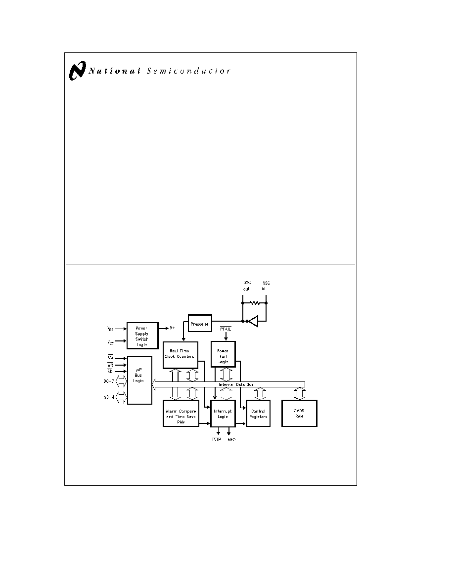
Block Diagram
TL F 11417 ≠ 1
FIGURE 1
TRI-STATE
is a registered trademark of National Semiconductor Corporation
C1995 National Semiconductor Corporation
RRD-B30M105 Printed in U S A
Absolute Maximum Ratings
(Notes 1
2)
Specifications for the 883 version of this product are
listed separately
Supply Voltage (V
CC
)
b
0 5V to
a
7 0V
DC Input Voltage (V
IN
)
b
0 5V to V
CC
a
0 5V
DC Output Voltage (V
OUT
)
b
0 5V to V
CC
a
0 5V
Storage Temperature Range
b
65 C to
a
150 C
Power Dissipation (PD)
500 mW
Lead Temperature (Soldering 10 sec )
260 C
Operation Conditions
Min
Max
Unit
Supply Voltage (V
CC
) (Note 3)
3 0
3 6
V
Supply Voltage (V
BB
) (Note 3)
2 2 V
CC
b
0 4
V
DC Input or Output Voltage
0 0
V
CC
V
(V
IN
V
OUT
)
Operation Temperature (T
A
)
b
40
a
85
C
Electr-Static Discharge Rating
1
kV
Typical Values
i
JA
DIP
Board
61 C W
Socket
67 C W
i
JA
PLCC
Board
80 C W
Socket
88 C W
DC Electrical Characteristics
V
CC
e
3 3V
g
10% V
BB
e
2 5V V
PFAIL
l
V
IH
C
L
e
100 pF (unless otherwise specified)
Symbol
Parameter
Conditions
Min
Max
Units
V
IH
High Level Input Voltage
Any Inputs Except OSC IN
2 0
V
CC
a
0 3
V
(Note 4)
OSC IN with External Clock
V
BB
b
0 2
V
V
IL
Low Level Input Voltage
All Inputs Except OSC IN
b
0 3
0 8
V
OSC IN with External Clock
b
0 3
0 2
V
V
OH
High Level Output Voltage
I
OUT
e b
20 mA
V
CC
b
0 2
V
(Excluding OSC OUT INTR)
I
OUT
e b
2 0 mA
2 4
V
V
OL
Low Level Output Voltage
I
OUT
e
20 mA
0 2
V
(Excluding OSC OUT)
I
OUT
e
2 0 mA
0 3
V
I
IN
Input Current (Except OSC IN)
V
IN
e
V
CC
or GND
g
0 7
m
A
I
OZ
Output TRI-STATE Current
V
OUT
e
V
CC
or GND
g
1
m
A
I
LKG
Output High Leakage Current
V
OUT
e
V
CC
or GND
g
1
m
A
MFO INTR Pins
Outputs Open Drain
I
CC
Quiescent Supply Current
F
OSC
e
32 768 kHz
(Note 7)
V
IN
e
V
CC
or GND (Note 5)
220
m
A
V
IN
e
V
CC
or GND (Note 6)
700
m
A
V
IN
e
V
IH
or V
IL
(Note 6)
5
mA
F
OSC
e
4 194304 MHz or
4 9152 MHz
V
IN
e
V
CC
or GND (Note 6)
4
mA
V
IN
e
V
IH
or V
IL
(Note 6)
6
mA
I
CC
Quiescent Supply Current
V
BB
e
GND
(Single Supply Mode)
V
IN
e
V
CC
or GND
(Note 7)
F
OSC
e
32 768 kHz
30
m
A
F
OSC
e
4 9152 MHz or
3
mA
4 194304 MHz
I
BB
Standby Mode Battery
V
CC
e
GND
Supply Current
OSC OUT
e
open circuit
(Note 7)
other pins
e
GND
F
OSC
e
32 768 kHzmA
8
m
A
F
OSC
e
4 9152 MHz or
400
m
A
4 194304 MHz
I
BLK
Battery Leakage
2 2V
s
V
BB
s
2 6V
other pins at GND
V
CC
e
GND V
BB
e
2 6V
0 8
m
A
V
CC
e
3 6V V
BB
e
2 2V
b
0 8
m
A
Note 1
Absolute Maximum Ratings are those values beyond which damage to the device may occur
Note 2
Unless otherwise specified all voltages are referenced to ground
Note 3
For F
OSC
e
4 194304 or 4 9152 MHz V
BB
minimum
e
2 8V In battery backed mode V
BB
s
V
CC
b
0 4V
Single Supply Mode Data retention voltage is 2 2V min
In single Supply Mode (Power connected to V
CC
pin) 3 0V
s
V
CC
s
3 6
Note 4
This parameter (V
IH
) is not tested on all pins at the same time
Note 5
This specification tests I
CC
with all power fail circuitry disabled by setting D7 of Interrupt Control Register 1 to 0
Note 6
This specification tests I
CC
with all power fail circuitry enabled by setting D7 of Interrupt Control Register 1 to 1
Note 7
OSC IN is driven by a signal generator Contents of the Test Register
e
00(H) and the MFO pin is not configured as buffered oscillator out
2
AC Electrical Characteristics
V
CC
e
3 3V
g
10% V
BB
e
2 5V V
PFAIL
l
V
IH
C
L
e
100 pF (unless otherwise specified)
Symbol
Parameter
Min
Max
Units
READ TIMING
t
AR
Address Valid Prior to Read Strobe
10
ns
t
RW
Read Strobe Width (Note 8)
100
ns
t
CD
Chip Select to Data Valid Time
100
ns
t
RAH
Address Hold after Read (Note 9)
2
ns
t
RD
Read Strobe to Valid Data
90
ns
t
DZ
Read or Chip Select to TRI-STATE
80
ns
t
RCH
Chip Select Hold after Read Strobe (Note 9)
0
ns
t
DS
Minimum Inactive Time between Read or Write Accesses
70
ns
WRITE TIMING
t
AW
Address Valid before Write Strobe
10
ns
t
WAH
Address Hold after Write Strobe (Note 9)
2
ns
t
CW
Chip Select to End of Write Strobe
110
ns
t
WW
Write Strobe Width (Note 10)
100
ns
t
DW
Data Valid to End of Write Strobe
70
ns
t
WDH
Data Hold after Write Strobe (Note 9)
2
ns
t
WCH
Chip Select Hold after Write Strobe (Note 9)
0
ns
INTERRUPT TIMING
t
ROLL
Clock Rollover to INTR Out is Typically 20 ms
Note 8
Read Strobe width as used in the read timing table is defined as the period when both chip select and read inputs are low Hence read commences when
both signals are low and terminates when either signal returns high
Note 9
Hold time is guaranteed by design but not production tested This limit is not used to calculate outgoing quality levels
Note 10
Write Strobe width as used in the write timing table is defined as the period when both chip select and write inputs are low Hence write commences when
both signals are low and terminates when either signal returns high
AC Test Conditions
Input Pulse Levels
GND to 3 0V
Input Rise and Fall Times
6 ns (10% ≠ 90%)
Input and Output
1 3V
Reference Levels
TRI-STATE Reference
Active High
a
0 5V
Levels (Note 12)
Active Low
b
0 5V
Note 11
C
L
e
100 pF includes jig and scope capacitance
Note 12
S1
e
V
CC
for active low to high impedance measurements
S1
e
GND for active high to high impedance measurements
S1
e
open for all other timing measurements
Capacitance
(T
A
e
25 C f
e
1 MHz)
Symbol
Parameter
Typ
Units
(Note 13)
C
IN
Input Capacitance
5
pF
C
OUT
Output Capacitance
7
pF
Note 13
This parameter is not 100% tested
Note 14
Output rise and fall times 25 ns max (10%≠90%) with 100 pF load
TL F 11417 ≠ 2
3
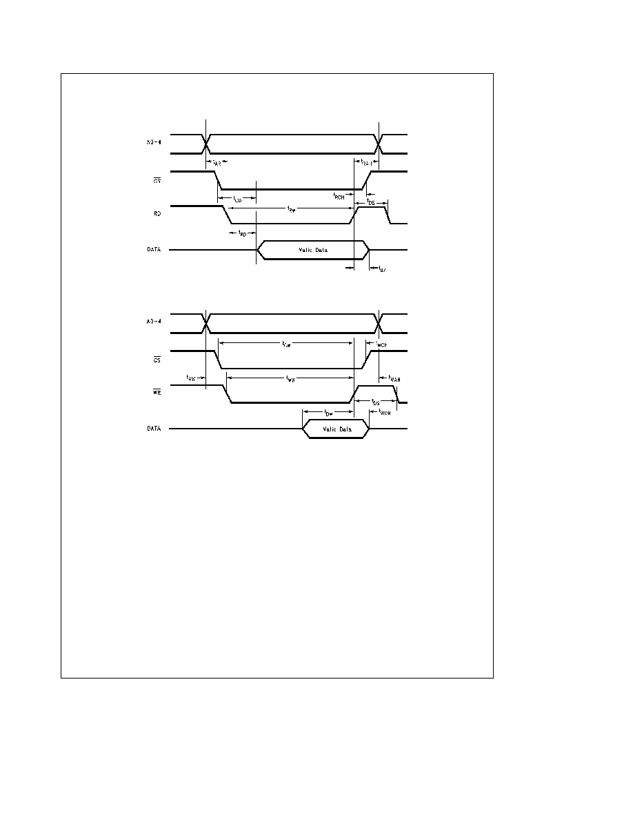
Timing Waveforms
Read Timing Diagram
TL F 11417 ≠ 3
Write Timing Diagram
TL F 11417 ≠ 4
4
General Description
(Continued)
The LV8572A's interrupt structure provides three basic
types of interrupts Periodic Alarm Compare and Power
Fail Interrupt mask and status registers enable the masking
and easy determination of each interrupt
Pin Description
CS RD WR (Inputs)
These pins interface to mP control
lines The CS pin is an active low enable for the read and
write operations Read and Write pins are also active low
and enable reading or writing to the RTC All three pins are
disabled when power failure is detected However if a read
or write is in progress at this time it will be allowed to com-
plete its cycle
A0 ≠ A4 (Inputs)
These 5 pins are for register selection
They individually control which location is to be accessed
These inputs are disabled when power failure is detected
OSC IN (Input) OSC OUT (Output)
These two pins are
used to connect the crystal to the internal parallel resonant
oscillator The oscillator is always running when power is
applied to V
BB
and V
CC
and the correct crystal select bits in
the Real Time Mode Register have been set
MFO (Output)
The multi-function output can be used as a
second interrupt output for interrupting the mP This pin can
also provide an output for the oscillator The MFO output is
configured as push-pull active high for normal or single
power supply operation and as an open drain during stand-
by mode (V
BB
l
V
CC
) If in battery backed mode and a pull-
up resistor is attached it should be connected to a voltage
no greater than V
BB
INTR (Output)
The interrupt output is used to interrupt the
processor when a timing event or power fail has occurred
and the respective interrupt has been enabled The INTR
output is permanently configured active low open drain If in
battery backed mode and a pull-up resistor is attached it
should be connected to a voltage no greater than V
BB
D0 ≠ D7 (Input Output)
These 8 bidirectional pins connect
to the host mP's data bus and are used to read from and
write to the RTC When the PFAIL pin goes low and a write
is not in progress these pins are at TRI-STATE
PFAIL (Input)
In battery backed mode this pin can have a
digital signal applied to it via some external power detection
logic When PFAIL
e
logic 0 the RTC goes into a lockout
mode in a minimum of 30 ms or a maximum of 63 ms unless
lockout delay is programmed In the single power supply
mode this pin is not useable as an input and should be tied
to V
CC
Refer to section on Power Fail Functional Descrip-
tion
V
BB
(Battery Power Pin)
This pin is connected to a back-
up power supply This power supply is switched to the inter-
nal circuitry when the V
CC
becomes lower than V
BB
Utiliz-
ing this pin eliminates the need for external logic to switch in
and out the back-up power supply If this feature is not to be
used then this pin must be tied to ground the RTC pro-
grammed for single power supply only and power applied to
the V
CC
pin
V
CC
This is the main system power pin
GND
This is the common ground power pin for both V
BB
and V
CC
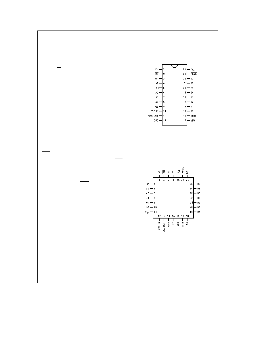
Connection Diagrams
In-Line Packages
TL F 11417 ≠ 5
Top View
DIP Order Number LV8572AN
See NS Package Number N24C
SOIC Order Number LV8572AM
See NS Package Number M24B
Plastic Chip Carrier
TL F 11417 ≠ 6
Top View
Order Number LV8572AV
See NS Package Number V28A
5