DS90LV001
3.3V LVDS-LVDS Buffer
General Description
The DS90LV001 LVDS-LVDS Buffer takes an LVDS input
signal and provides an LVDS output signal. In many large
systems, signals are distributed across backplanes, and one
of the limiting factors for system speed is the 'stub length' or
the distance between the transmission line and the untermi-
nated receivers on individual cards. Although it is generally
recognized that this distance should be as short as possible
to maximize system performance, real-world packaging con-
cerns often make it difficult to make the stubs as short as the
designer would like.
The DS90LV001, available in the LLP (Leadless Leadframe
Package) package, will allow the receiver to be placed very
close to the main transmission line, thus improving system
performance.
A wide input dynamic range will allow the DS90LV001 to
receive differential signals from LVPECL as well as LVDS
sources. This will allow the device to also fill the role of an
LVPECL-LVDS translator.
An output enable pin is provided, which allows the user to
place the LVDS output in TRI-STATE.
The DS90LV001 is offered in two package options, an 8 pin
LLP and SOIC.
Features
n
Single +3.3 V Supply
n
LVDS receiver inputs accept LVPECL signals
n
TRI-STATE outputs
n
Receiver input threshold
<
±
100 mV
n
Fast propagation delay of 1.4 ns (typ)
n
Low jitter 800 Mbps fully differential data path
n
100 ps (typ) of pk-pk jitter with PRBS = 2
23
-1 data
pattern at 800 Mbps
n
Compatible with ANSI/TIA/EIA-644-A LVDS standard
n
8 pin SOIC and space saving (70%) LLP package
n
Industrial Temperature Range
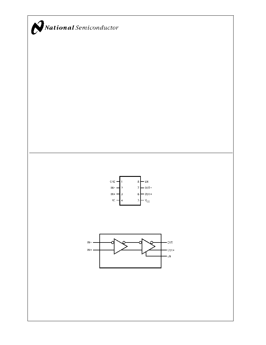
Connection Diagram
Block Diagram
Top View
DS101338-5
Order Number DS90LV001TM, DS90LV001TLD
See NS Package Number M08A, LDA08A
DS101338-2
April 2001
DS90L
V001
3.3V
L
VDS-L
VDS
Buffer
© 2001 National Semiconductor Corporation
DS101338
www.national.com
Absolute Maximum Ratings
(Note 1)
If Military/Aerospace specified devices are required,
please contact the National Semiconductor Sales Office/
Distributors for availability and specifications.
Supply Voltage (V
CC
)
-0.3V to +4V
LVCMOS/LVTTL Input Voltage
(EN)
-0.3V to (V
CC
+ 0.3V)
LVDS Receiver Input Voltage
(IN+, IN-)
-0.3V to +4V
LVDS Driver Output Voltage
(OUT+, OUT-)
-0.3V to +4V
LVDS Output Short Circuit
Current
Continuous
Junction Temperature
+150∞C
Storage Temperature Range
-65∞C to +150∞C
Lead Temperature Range
Soldering (4 sec.)
+260∞C
Maximum Package Power Dissipation at 25∞C
M Package
726 mW
Derate M Package
5.8 mW/∞C above +25∞C
LDA Package
2.44 W
Derate LDA Package
19.49 mW/∞C above
+25∞C
ESD Ratings
(HBM, 1.5k
, 100pF)
2.5kV
(EIAJ, 0
, 200pF)
250V
Recommended Operating
Conditions
Min
Typ
Max
Units
Supply Voltage (V
CC
)
3.0
3.3
3.6
V
Receiver Input Voltage
0
V
CC
V
Operating Free Air
Temperature
-40
+25
+85
∞C
Electrical Characteristics
Over recommended operating supply and temperature ranges unless otherwise specified. (Notes 2, 3)
Symbol
Parameter
Conditions
Min
Typ
Max
Units
LVCMOS/LVTTL DC SPECIFICATIONS (EN)
V
IH
High Level Input Voltage
2.0
V
CC
V
V
IL
Low Level Input Voltage
GND
0.8
V
I
IH
High Level Input Current
V
IN
= 3.6V or 2.0V, V
CC
= 3.6V
+7
+20
µA
I
IL
Low Level Input Current
V
IN
= GND or 0.8V, V
CC
= 3.6V
±
1
±
10
µA
V
CL
Input Clamp Voltage
I
CL
= -18 mA
-0.6
-1.5
V
LVDS OUTPUT DC SPECIFICATIONS (OUT)
V
OD
Differential Output Voltage
R
L
= 100
250
325
450
mV
V
OD
Change in Magnitude of V
OD
for Complimentary
Output States
Figure 1 and Figure 2
20
mV
V
OS
Offset Voltage
R
L
= 100
1.080
1.19
1.375
V
V
OS
Change in Magnitude of V
OS
for Complimentary
Output States
Figure 1
20
mV
I
OZ
Output TRI-STATE Current
EN = 0V, V
OUT
= V
CC
or GND
±
1
±
10
µA
I
OFF
Power-Off Leakage Current
V
CC
= 0V, V
OUT
= 3.6V or GND
±
1
±
10
µA
I
OS
Output Short Circuit Current (Note 4)
EN = V
CC
, V
OUT+
and V
OUT-
= 0V
-16
-24
mA
I
OSD
Differential Output Short Circuit Current (Note 4)
EN = V
CC
, V
OD
= 0V
-7
-12
mA
LVDS RECEIVER DC SPECIFICATIONS (IN)
V
TH
Differential Input High Threshold
V
CM
= +0.05V, +1.2V or +3.25V
0
+100
mV
V
TL
Differential Input Low Threshold
-100
0
mV
V
CMR
Common Mode Voltage Range
V
ID
= 100mV, V
CC
= 3.3V
0.05
3.25
V
I
IN
Input Current
V
IN
= +3.0V
V
CC
= 3.6V or 0V
±
1
±
10
µA
V
IN
= 0V
±
1
±
10
µA
I
IN
Change in Magnitude of I
IN
V
IN
= +3.0V
V
CC
= 3.6V or 0V
1
6
µA
V
IN
= 0V
1
6
µA
SUPPLY CURRENT
I
CCD
Total Supply Current
EN = V
CC
, R
L
= 100
, C
L
= 5 pF
47
70
mA
I
CCZ
TRI-STATE Supply Current
EN = 0V
22
35
mA
DS90L
V001
www.national.com
2
AC Electrical Characteristics
Over recommended operating supply and temperature ranges unless otherwise specified. (Note 3)
Symbol
Parameter
Conditions
Min
Typ
Max
Units
t
PHLD
Differential Propagation Delay High to Low
R
L
= 100
, C
L
= 5pF
1.0
1.4
2.0
ns
t
PLHD
Differential Propagation Delay Low to High
Figure 3 and Figure 4
1.0
1.4
2.0
ns
t
SKD1
Pulse Skew |t
PLHD
- t
PHLD
| (Note 5) (Note 6)
20
200
ps
t
SKD3
Part to Part Skew (Note 5) (Note 7)
0
60
ps
t
SKD4
Part to Part Skew (Note 5) (Note 8)
400
ps
t
LHT
Rise Time (Note 5)
R
L
= 100
, C
L
= 5pF
200
320
450
ps
t
HLT
Fall Time (Note 5)
Figure 3 and Figure 5
200
310
450
ps
t
PHZ
Disable Time (Active High to Z)
R
L
= 100
, C
L
= 5pF
3
25
ns
t
PLZ
Disable Time (Active Low to Z)
Figure 6 and Figure 7
3
25
ns
t
PZH
Enable Time (Z to Active High)
25
45
ns
t
PZL
Enable Time (Z to Active Low)
25
45
ns
t
DJ
LVDS Data Jitter, Deterministic (Peak-to-Peak)
(Note 9)
V
ID
= 300mV; PRBS = 2
23
- 1 data;
V
CM
= 1.2V at 800Mbps (NRZ)
100
135
ps
t
RJ
LVDS Clock Jitter, Random (Note 9)
V
ID
= 300mV; V
CM
= 1.2V at 400MHz
clock
2.2
3.5
ps
Note 1: "Absolute Maximum Ratings" are those values beyond which the safety of the device cannot be guaranteed. They are not meant to imply that the device
should be operated at these limits. The table of "Electrical Characteristics" specifies conditions of device operation.
Note 2: Current into device pins is defined as positive. Current out of device pins is defined as negative. All voltages are referenced to ground except V
OD
and
V
OD
.
Note 3: All typical are given for V
CC
= +3.3V and T
A
= +25∞C, unless otherwise stated.
Note 4: Output short circuit current (I
OS
) is specified as magnitude only, minus sign indicates direction only.
Note 5: The parameters are guaranteed by design. The limits are based on statistical analysis of the device performance over the PVT (process, voltage and
temperature) range.
Note 6: t
SKD1
, |t
PLHD
- t
PHLD
|, is the magnitude difference in differential propagation delay time between the positive going edge and the negative going edge of
the same channel.
Note 7: t
SKD3
, Part to Part Skew, is defined as the difference between the minimum and maximum specified differential propagation delays. This specification
applies to devices at the same V
CC
and within 5∞C of each other within the operating temperature range.
Note 8: t
SKD4
, Part to Part Skew, is the differential channel-to- channel skew of any event between devices. This specification applies to devices over recommended
operating temperature and voltage ranges, and across process distribution. t
SKD4
is defined as |Max - Min| differential propagation delay.
Note 9: The parameters are guaranteed by design. The limits are based on statistical analysis of the device performance over the PVT range with the following test
equipment setup: HP8133A (pattern pulse generator), 5 feet of RG142B cable with DUT test board and HP83480A (digital scope mainframe) with HP83484A (50GHz
scope module). The HP8133A with RG142B cable exhibit a t
DJ
= 21ps and t
RJ
= 1.8ps.
DS90L
V001
www.national.com
3
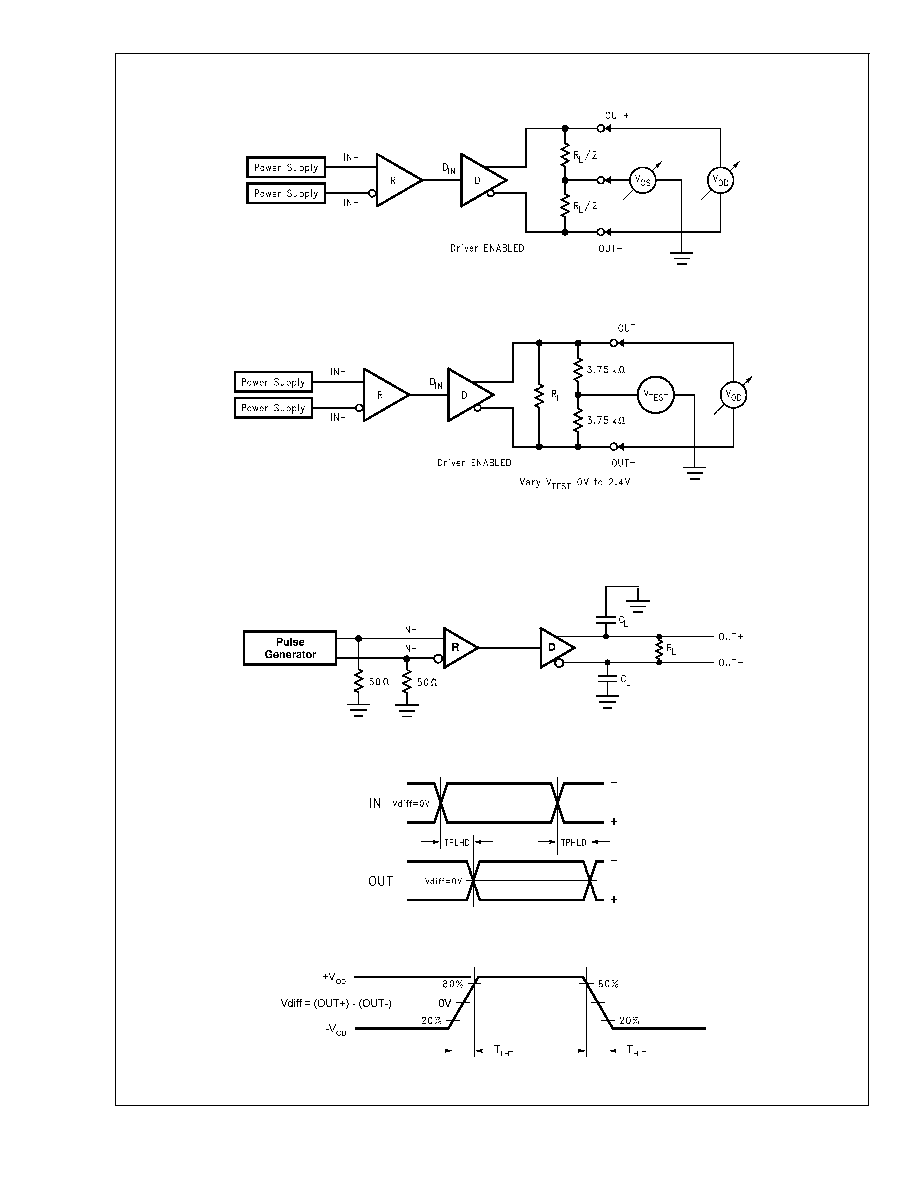
DC Test Circuits
AC Test Circuits and Timing Diagrams
DS101338-3
FIGURE 1. Differential Driver DC Test Circuit
DS101338-8
FIGURE 2. Differential Driver Full Load DC Test Circuit
DS101338-6
FIGURE 3. LVDS Output Load
DS101338-7
FIGURE 4. Propagation Delay Low-to-High and High-to-Low
DS101338-9
FIGURE 5. LVDS Output Transition Time
DS90L
V001
www.national.com
4
AC Test Circuits and Timing Diagrams
(Continued)
DS101338-1
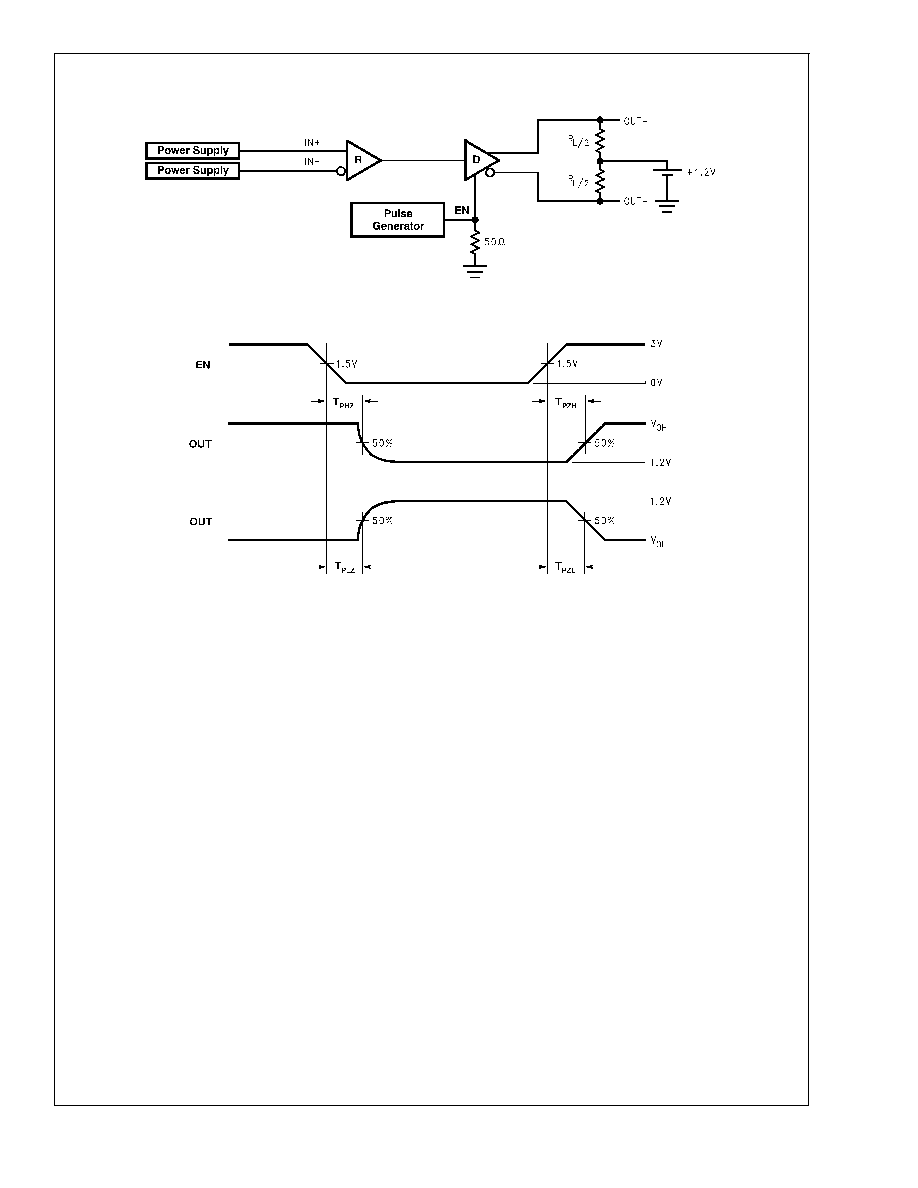
FIGURE 6. TRI-STATE Delay Test Circuit
DS101338-4
FIGURE 7. Output active to TRI-STATE and TRI-STATE to active output time
DS90L
V001
www.national.com
5