 | –≠–ª–µ–∫—Ç—Ä–æ–Ω–Ω—ã–π –∫–æ–º–ø–æ–Ω–µ–Ω—Ç: M08A | –°–∫–∞—á–∞—Ç—å:  PDF PDF  ZIP ZIP |

LM4991
3W Audio Power Amplifier with Shutdown Mode
General Description
The LM4991 is a mono bridged audio power amplifier ca-
pable of delivering 3W of continuous average power into a
3
load with less than 10% THD when powered by a 5V
power supply (Note 1). To conserve power in portable appli-
cations, the LM4991's micropower shutdown mode (I
SD
=
0.1µA, typ) is activated when V
DD
is applied to the SHUT-
DOWN pin.
Boomer audio power amplifiers are designed specifically to
provide high power, high fidelity audio output. They require
few external components and operate on low supply volt-
ages from 2.2V to 5.5V. Since the LM4991 does not require
output coupling capacitors, bootstrap capacitors, or snubber
networks, it is ideally suited for low-power portable systems
that require minimum volume and weight.
Additional LM4991 features include thermal shutdown pro-
tection, unity-gain stability, and external gain set.
Note 1: An LM4991LD that has been properly mounted to a circuit board will
deliver 3W into 3
(at 10% THD). The other package options for the LM4991
will deliver 1.5W into 8
(at 10% THD). See the Application Information
sections for further information concerning the LM4991LD and LM4991M.
Key Specifications
n
Improved PSRR at 217kHz and 1kHz
64dB (typ)
n
P
O
at V
DD
= 5.0V, 10% THD, 1kHz
n
LM4991LD (only), 3
, 4
3W (typ), 2.5W (typ)
n
All packages, 8
load
1.5W (typ)
n
Shutdown current
0.1µA (typ)
Features
n
Available in space-saving LLP and MA packages
n
Ultra low current shutdown mode
n
Can drive capacitive loads up to 500pF
n
Improved pop & click circuitry reduces noises during
turn-on and turn-off transitions
n
2.2 - 5.5V operation
n
No output coupling capacitors, snubber networks,
bootstrap capacitors or gain-setting resistors required
n
Unity-gain stable
Applications
n
Wireless and cellular handsets
n
PDA's
n
Portable computers
n
Desktop computers
Connection Diagrams
Small Outline Package
LLP Package
20074002
Top View
Order Number LM4991MA
See NS Package Number M08A
20074039
Top View
Order Number LM4991LD
See NS Package Number LDC08A
Boomer
Æ
is a registered trademark of National Semiconductor Corporation.
May 2003
LM4991
3W
Audio
Power
Amplifier
with
Shutdown
Mode
© 2003 National Semiconductor Corporation
DS200740
www.national.com

Typical Application
20074001
FIGURE 1. Typical Audio Amplifier Application Circuit
LM4991
www.national.com
2

Absolute Maximum Ratings
(Note 2)
If Military/Aerospace specified devices are required,
please contact the National Semiconductor Sales Office/
Distributors for availability and specifications.
Supply Voltage
6.0V
Supply Temperature
-65∞C to +150∞C
Input Voltage
-0.3V to V
DD
to +0.3V
Power Dissipation (Note 4)
Internally Limited
ESD Susceptibility (Note 5)
2000V
ESD Susceptibility (Note 6)
200V
Junction Temperature
150∞C
Thermal Resistance
JC
(LD) (Note 9)
4.3∞C/W
JA
(LD)
56∞C/W
JC
(MA)
35∞C/W
JA
(MA)
140∞C/W
Operating Ratings
Temperature Range
T
MIN
T
A
T
MAX
-40∞C
T
A
+85∞C
Supply Voltage
2.2V
V
DD
5.5V
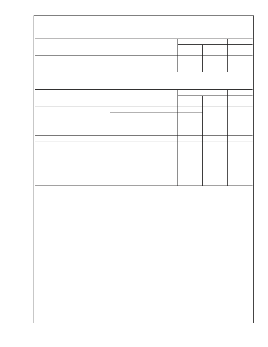
Electrical Characteristics V
DD
= 5V
(Notes 2, 3)
The following specifications apply for V
DD
= 5V and R
L
= 8
unless otherwise specified. Limits apply for T
A
= 25∞C.
Symbol
Parameter
Conditions
LM4991
Typical
(Note 7)
Limit
(Note 8)
Units
(Limits)
I
DD
Quiescent Power Supply
Current
V
IN
= 0V, no Load
3
7
mA (max)
V
IN
= 0V, R
L
= 8
4
10
I
SD
Shutdown Current
V
SHUTDOWN
= V
DD
0.1
2.0
µA (max)
V
SDIH
Shutdown Voltage
1.5
V
V
SDIL
1.3
V
V
OS
Output Offset Voltage
5
35
mV (max)
P
o
Output Power
THD = 1% (max), f = 1kHz
LM4991LD, R
L
= 3
(Note 10)
LM4991LD, R
L
= 4
(Note 10)
LM4991, R
L
= 8
2.38
2.1
1.3
0.9
W (min)
THD+N = 10%, f = 1kHz
LM4991LD, R
L
= 3
(Note 10)
LM4991LD, R
L
= 4
(Note 10)
LM4991, R
L
= 8
3
2.5
1.5
W
THD+N
Total Harmonic
Distortion+Noise
P
O
= 0.5W, f = 1kHz
0.2
%
PSRR
Power Supply Rejection
Ratio
V
RIPPLE
= 200mV sine p-p,
Input terminated with 10
,
f = 1kHz
64
55
dB (min)
Electrical Characteristics V
DD
= 3V
(Notes 2, 3)
The following specifications apply for V
DD
= 3V and R
L
= 8
unless otherwise specified. Limits apply for T
A
= 25∞C.
Symbol
Parameter
Conditions
LM4991
Typical
(Note 7)
Limit
(Note 8)
Units
(Limits)
I
DD
Quiescent Power Supply
Current
V
IN
= 0V, no Load
3
7
mA (max)
V
IN
= 0V, R
L
= 8
4
7
I
SD
Shutdown Current
V
SHUTDOWN
= V
DD
0.1
2.0
µA (max)
V
SDIH
Shutdown Voltage Input High
1.1
V
V
SDIL
Shutdown Voltage Input Low
0.9
V
V
OS
Output Offset Voltage
5
35
mV (max)
P
o
Output Power
THD = 1% (max), f = 1kHz
R
L
= 4
R
L
= 8
600
425
mW
THD+N
Total Harmonic
Distortion+Noise
P
O
= 0.25W, f = 1kHz
0.1
%
LM4991
www.national.com
3
Electrical Characteristics V
DD
= 3V
(Notes 2, 3)
The following specifications apply for V
DD
= 3V and R
L
= 8
unless otherwise specified. Limits apply for T
A
=
25∞C. (Continued)
Symbol
Parameter
Conditions
LM4991
Typical
(Note 7)
Limit
(Note 8)
Units
(Limits)
PSRR
Power Supply Rejection
Ratio
V
RIPPLE
= 200mV sine p-p,
Input terminated with 10
,
f = 1kHz
68
dB
Electrical Characteristics V
DD
= 2.6V
(Notes 2, 3)
The following specifications apply for V
DD
= 2.6V and R
L
= 8
unless otherwise specified. Limits apply for T
A
= 25∞C.
Symbol
Parameter
Conditions
LM4991
Typical
(Note 7)
Limit
(Note 8)
Units
(Limits)
I
DD
Quiescent Power Supply
Current
V
IN
= 0V, no Load
2
mA (max)
V
IN
= 0V, R
L
= 8
3
I
SD
Shutdown Current
V
SHUTDOWN
= V
DD
0.1
µA(max)
V
SDIH
Shutdown Voltage Input High
1
V
V
SDIL
Shutdown Voltage Input Low
0.9
V
V
OS
Output Offset Voltage
5
35
mV (max)
P
o
Output Power
THD = 1% (max), f = 1kHz
R
L
= 4
R
L
= 8
400
300
mW
THD+N
Total Harmonic
Distortion+Noise
P
O
= 0.15W, f = 1kHz
0.1
%
PSRR
Power Supply Rejection
Ratio
V
RIPPLE
= 200mV sine p-p,
Input terminated with 10
,
f = 1kHz
51
dB
Note 2: Absolute Maximum Ratings indicate limits beyond which damage to the device may occur. Operating Ratings indicate conditions for which the device is
functional, but do not guarantee specific performance limits. Electrical Characteristics state DC and AC electrical specifications under particular test conditions which
guarantee specific performance limits. This assumes that the device is within the Operating Ratings. Specifications are not guaranteed for parameters where no limit
is given, however, the typical value is a good indication of device performance.
Note 3: All voltages are measured with respect to the ground pin, unless otherwise specified.
Note 4: The maximum power dissipation must be derated at elevated temperatures and is dictated by T
JMAX
,
JA
, and the ambient temperature T
A
. The maximum
allowable power dissipation is P
DMAX
= (T
JMAX
≠T
A
)/
JA
or the number given in Absolute Maximum Ratings, whichever is lower. For the LM4991, T
JMAX
= 150∞C.
For the
JA
's for different packages, please see the Application Information section or the Absolute Maximum Ratings section.
Note 5: Human body model, 100pF discharged through a 1.5k
resistor.
Note 6: Machine Model, 220pF≠240pF discharged through all pins.
Note 7: Typicals are specified at 25∞C and represent the parametric norm.
Note 8: Limits are guaranteed to National's AOQL (Average Outgoing Quality Level).
Note 9: The given
JA
is for an LM4991 packaged in an LDC08A with the Exposed≠DAP soldered to an exposed 1in
2
area of 1oz printed circuit board copper.
Note 10: When driving 3
or 4 loads from a 5V supply, the LM4991LD must be mounted to a circuit board.
LM4991
www.national.com
4

External Components Description
(Figure 1)
Components
Functional Description
1.
R
i
Inverting input resistance that sets the closed-loop gain in conjunction with R
f
. This resistor also forms a high
pass filter with C
i
at f
C
= 1/(2
R
i
C
i
).
2.
C
i
Input coupling capacitor that blocks the DC voltage at the amplifiers input terminals. Also creates a highpass
filter with R
i
at f
c
= 1/(2
R
i
C
i
). Refer to the section, Proper Selection of External Components, for an
explanation of how to determine the value of C
i
.
3.
R
f
Feedback resistance that sets the closed-loop gain in conjunction with R
i
.
4.
C
S
Supply bypass capacitor that provides power supply filtering. Refer to the Power Supply Bypassing section
for information concerning proper placement and selection of the supply bypass capacitor.
5.
C
B
Bypass pin capacitor that provides half-supply filtering. Refer to the section, Proper Selection of External
Components, for information concerning proper placement and selection of C
B
.
Typical Performance Characteristics
LD and MH Specific Characteristics
THD+N vs Frequency
V
DD
= 5V, R
L
= 4
, and P
O
= 1W
THD+N vs Output Power
V
DD
= 5V, R
L
= 4
, and f = 1 kHz
20074041
20074042
Typical Performance Characteristics
THD+N vs Frequency
V
DD
= 5V, R
L
= 8
, and P
O
= 500mW
THD+N vs Frequency
V
DD
= 3V, R
L
= 4
, and P
O
= 500mW
20074043
20074044
LM4991
www.national.com
5