 | –≠–ª–µ–∫—Ç—Ä–æ–Ω–Ω—ã–π –∫–æ–º–ø–æ–Ω–µ–Ω—Ç: MM74C903 | –°–∫–∞—á–∞—Ç—å:  PDF PDF  ZIP ZIP |
TL F 9786
54283DM74283
4-Bit
Binary
Full
Adder
(with
Fast
Carry)
June 1989
54283 DM74283
4-Bit Binary Full Adder (with Fast Carry)
General Description
The '283 high speed 4-bit binary full adders with internal
carry lookahead accept two 4-bit binary words (A0 ≠ A3 B0 ≠
B3) and a Carry input (C0) They generate the binary Sum
outputs (S0 ≠ S3) and the Carry output (C4) from the most
significant bit They operate with either active HIGH or ac-
tive LOW operands (positive or negative logic)
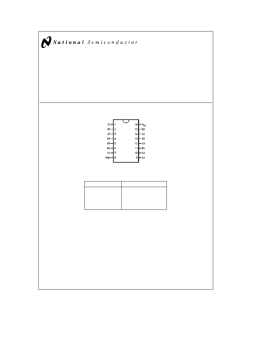
Connection Diagram
Dual-In-Line Package
TL F 9786 ≠ 1
Order Number 54283DMQB 54283FMQB or DM74283N
See NS Package Number J16A N16E or W16A
Pin Names
Description
A0 ≠ A3
A Operand Inputs
B0 ≠ B3
B Operand Inputs
C0
Carry Input
S0 ≠ S3
Sum Outputs
C4
Carry Output
C1995 National Semiconductor Corporation
RRD-B30M115 Printed in U S A
Absolute Maximum Ratings
(Note)
If Military Aerospace specified devices are required
please contact the National Semiconductor Sales
Office Distributors for availability and specifications
Supply Voltage
7V
Input Voltage
5 5V
Operating Free Air Temperature Range
54
b
55 C to
a
125 C
DM74
0 C to
a
70 C
Storage Temperature Range
b
65 C to
a
150 C
Note
The ``Absolute Maximum Ratings'' are those values
beyond which the safety of the device cannot be guaran-
teed The device should not be operated at these limits The
parametric values defined in the ``Electrical Characteristics''
table are not guaranteed at the absolute maximum ratings
The ``Recommended Operating Conditions'' table will define
the conditions for actual device operation
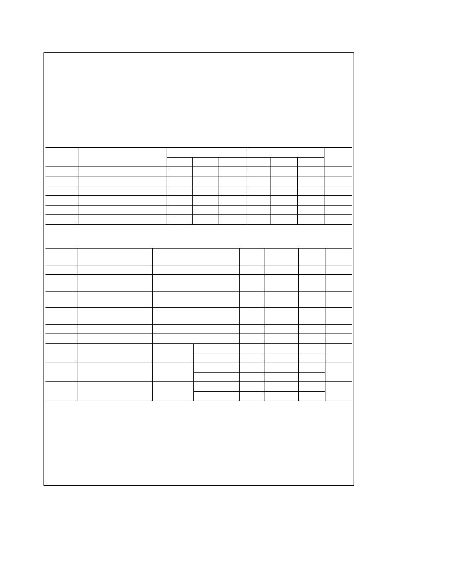
Recommended Operating Conditions
Symbol
Parameter
54283
DM74283
Units
Min
Nom
Max
Min
Nom
Max
V
CC
Supply Voltage
4 5
5
5 5
4 75
5
5 25
V
V
IH
High Level Input Voltage
2
2
V
V
IL
Low Level Input Voltage
0 8
0 8
V
I
OH
High Level Output Current
b
0 4
b
0 4
mA
I
OL
Low Level Output Current
16
16
mA
T
A
Free Air Operating Temperature
b
55
125
0
70
C
Electrical Characteristics
Over recommended operating free air temperature range (unless otherwise noted)
Symbol
Parameter
Conditions
Min
Typ
Max
Units
(Note 1)
V
I
Input Clamp Voltage
V
CC
e
Min I
I
e b
12 mA
b
1 5
V
V
OH
High Level Output Voltage
V
CC
e
Min I
OH
e
Max
2 4
3 4
V
V
IL
e
Max
V
OL
Low Level Output Voltage
V
CC
e
Min I
OL
e
Max
0 2
0 4
V
V
IH
e
Min
I
I
Input Current
Max
V
CC
e
Max V
I
e
5 5V
1
mA
Input Voltage
I
IH
High Level Input Current
V
CC
e
Max V
I
e
2 4V
40
m
A
I
IL
Low Level Input Current
V
CC
e
Max V
I
e
0 4V
b
1 6
mA
I
OS
Short Circuit
V
CC
e
Max
54
b
20
b
55
mA
Output Current at S
n
(Note 2)
DM74
b
20
b
55
I
OS
Short Circuit
V
CC
e
Max
54
b
20
b
70
mA
Output Current at C4
(Note 2)
DM74
b
18
b
70
I
CCH
Supply Current with
V
CC
e
Max
54
99
mA
Outputs High
DM74
110
Note 1
All typicals are at V
CC
e
5V T
A
e
25 C
Note 2
Not more than one output should be shorted at a time
2
Switching Characteristics
V
CC
e a
5 0V T
A
e a
25 C (See Section 1 for waveforms and load configurations)
Symbol
Parameter
C
L
e
15 pF R
L
e
400X
Units
Min
Max
t
PLH
Propagation Delay
21
ns
t
PHL
C0 or S
n
21
t
PLH
Propagation Delay
24
ns
t
PHL
A
n
or B
n
to S
n
24
t
PLH
Propagation Delay
14
ns
t
PHL
C0 to C4
16
t
PLH
Propagation Delay
14
ns
t
PHL
A
n
or B
n
to C4
16
Functional Description
The '283 adds two 4-bit binary words (A plus B) plus the
incoming carry C0 The binary sum appears on the Sum
(S0 ≠ S3) and outgoing carry (C4 outputs The binary weight
of the various inputs and outputs is indicated by the sub-
script numbers representing powers of two
2
0
(A0
a
B0
a
C0)
a
2
1
(A1
a
B1)
a
2
2
(A2
a
B2)
a
2
3
(A3
a
B3)
e
S0
a
2S1
a
4S2
a
8S3
a
16C4
Where (
a
)
e
plus
Interchanging inputs of equal weight does not affect the op-
eration Thus C0 A0 B0 can be arbitrarily assigned to pins
5 6 and 7 Due to the symmetry of the binary add function
the '283 can be used either with all inputs and outputs ac-
tive HIGH (positive logic) or with all inputs and outputs ac-
tive LOW (negative logic) Note that if C0 is not used it must
be tied LOW for active HIGH logic or tied HIGH for active
LOW logic
Example
C0 A0 A1 A2 A3 B0 B1 B2 B3 S0 S1 S2 S3 C4
Logic Levels L
L H L H H L
L H H H L L H
Active HIGH 0
0
1
0
1
1
0
0
1 1 1 0 0 1
Active LOW 1
1
0
1
0
0
1
1
0 0 0 1 1 0
Active HIGH 0
a
10
a
9
e
3
a
16
Active LOW 1
a
5
a
6
e
12
a
0
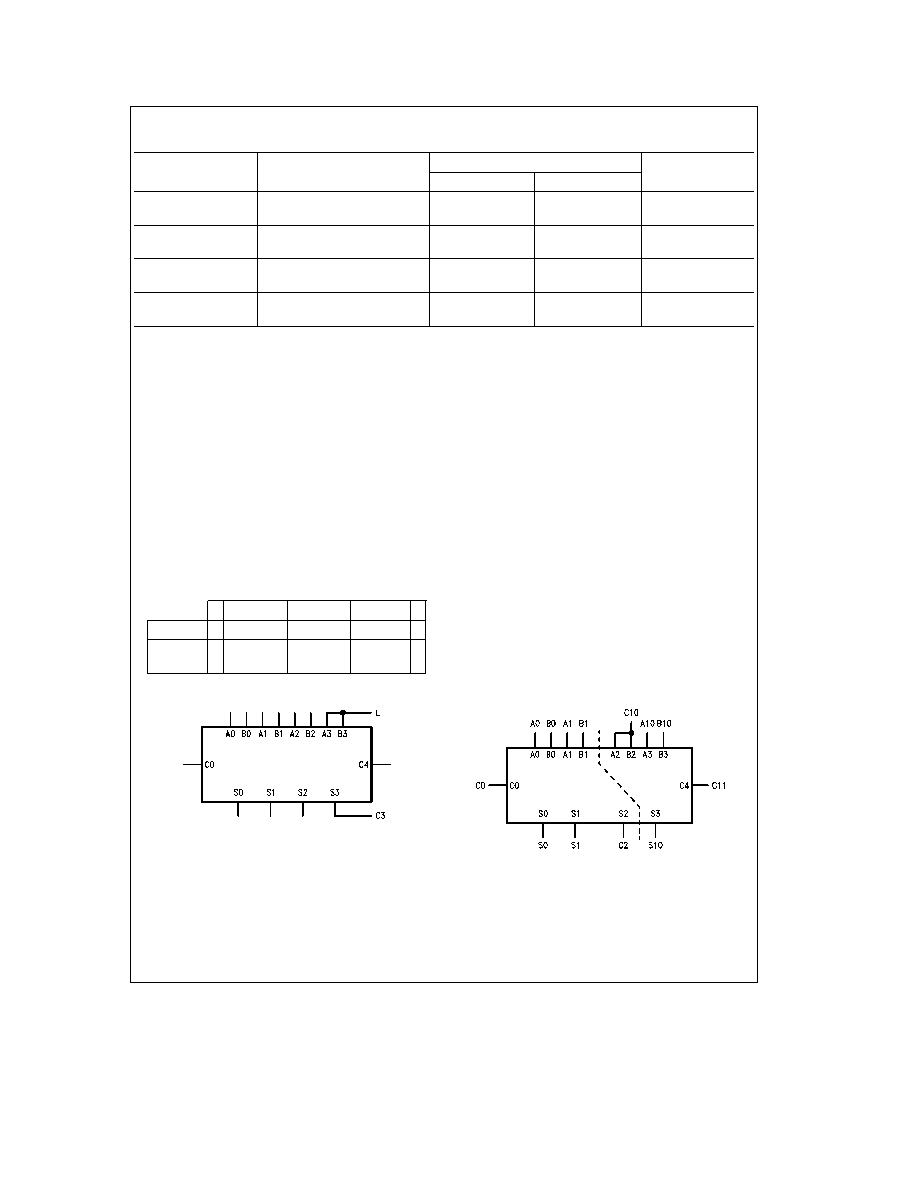
Due to pin limitations the intermediate carries of the '283
are not brought out for use as inputs or outputs However
other means can be used to effectively insert a carry into or
bring a carry out from an intermediate stage
Figure a
shows a way of making a 3-bit adder Tying the operand
inputs of the fourth adder (A3 B3) LOW makes S3 depen-
dent ony on and equal to the carry from the third adder
Using somewhat the same principle
Figure b shows a way
of dividing the '283 into a 2-bit and a 1-bit adder The third
stage adder (A2 B2 S2) is used merely as a means of
getting a carry (C10) signal into the fourth stage (via A2 and
B2) and bringing out the carry from the second stage on S2
Note that as long as A2 and B2 are the same whether
HIGH or LOW they do not infuence S2 Similarly when A2
and B2 are the same the carry into the third stage does not
influence they carry out of the third stage
Figure c shows a
method of implementing a 5-input encoder where the inputs
are equally weighted The outputs S0 S1 and S2 present a
binary number equal to the number of inputs I1 ≠ I5 that are
true
Figure d shows one method of implementing a 5-input
majority gate When three or more of the inputs I1 ≠ I5 are
true the output M5 is true
TL F 9786 ≠ 3
FIGURE a 3-Bit Adder
TL F 9786 ≠ 4
FIGURE b 2-Bit and 1-Bit Adders
3
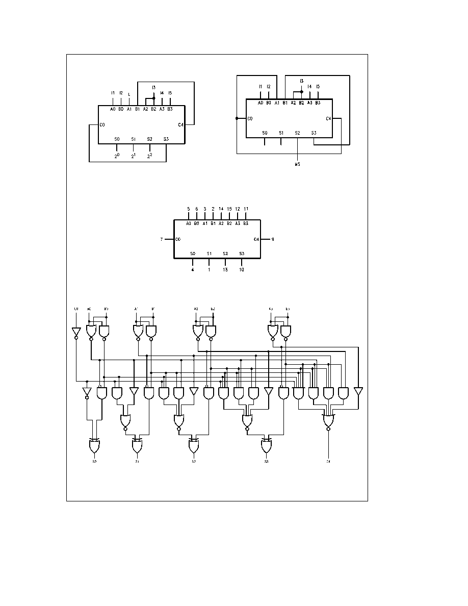
Functional Description
(Continued)
TL F 9786 ≠ 5
FIGURE c 5-Input Encoder
TL F 9786 ≠ 6
FIGURE d 5-Input Majority Gate
Logic Symbol
TL F 9786 ≠ 2
V
CC
e
Pin 16
GND
e
Pin 8
Logic Diagram
TL F 9786 ≠ 7
4
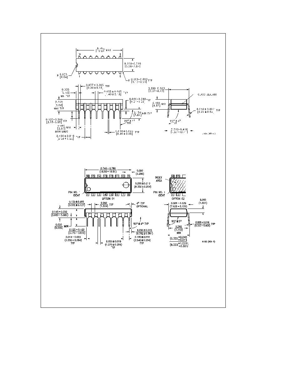
Physical Dimensions
inches (millimeters)
16-Lead Ceramic Dual-In-Line Package (J)
Order Number 54283DMQB
NS Package Number J16A
16-Lead Molded Dual-In-Line Package (N)
Order Number DM74283N
NS Package Number N16E
5