Original Creation Date: 04/14/00
Last Update Date: 08/15/03
Last Major Revision Date:
MNDS90C032-X-RH REV 1B1
MICROCIRCUIT DATA SHEET
LVDS Quad CMOS Differential Line Receiver: ALSO
AVAILABLE GUARANTEED TO 50K RAD(Si) TESTED TO
MIL-STD-883, METHOD 1019.5
General Description
The DS90C032 is a quad differential line receiver designed for applications requiring low
power dissipation and high data rates.
The DS90C032 accepts low voltage differential input siginal and translates them to CMOS
(TTL compatible) output levels. The receiver supports a TRI-STATE function that may be
used to multiplex outputs.
The DS90C032 and companion line driver (DS90C031) provide a new alternative to high power
pseudo-ECL devices for high speed point to point interfaces.
In addition, the DS90C032A provides power-off high impedance LVDS inputs. This feature
assures minimal loading effect on the LVDS bus lines when VCC is not present.
NS Part Numbers
DS90C032E-QML
DS90C032W-QML
DS90C032W-QMLV
DS90C032WG-QML
DS90C032WG-QMLV
DS90C032WGLQMLV
DS90C032WLQMLV
Industry Part Number
DS90C032
Prime Die
DS90C032
Controlling Document
SEE FEATURES SECTION
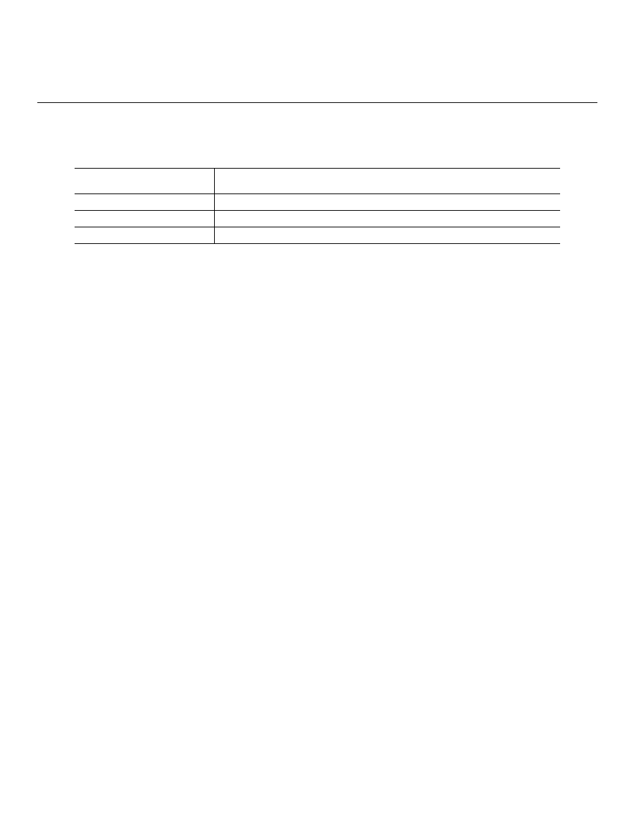
Processing
MIL-STD-883, Method 5004
Quality Conformance Inspection
MIL-STD-883, Method 5005
Subgrp Description Temp ( C)
o
1
Static tests at
+25
2
Static tests at
+125
3
Static tests at
-55
4
Dynamic tests at
+25
5
Dynamic tests at
+125
6
Dynamic tests at
-55
7
Functional tests at
+25
8A
Functional tests at
+125
8B
Functional tests at
-55
9
Switching tests at
+25
10
Switching tests at
+125
11
Switching tests at
-55
1

MICROCIRCUIT DATA SHEET
MNDS90C032-X-RH REV 1B1
Features
- High impedance LVDS inputs with power-off
- Accepts small swing (330 mV) differential signal levels.
- Low power dissipation.
- Low differential skew.
- Low chip to chip skew
- Mil operating temperature range
- Pin compatible with DS26C32A.
- Compatible with IEEE P1596.3 SCI LVDS draft standard
- Typical Rise/Fall time is TBD
CONTROLLING DOCUMENTS:
DS90C032E-QML 5962-9583401Q2A
DS90C032W-QML 5962-9583401QFA
DS90C032W-QMLV 5962-9583401VFA
DS90C032WG-QML 5962-9583401QZA
DS90C032WG-QMLV 5962-9583401VZA
DS90C032WGLQMLV 5962-9583401VZA
DS90C032WLQMLV 5962L9583401VFA
2

MICROCIRCUIT DATA SHEET
MNDS90C032-X-RH REV 1B1
(Absolute Maximum Ratings)
(Note 1)
Supply Voltage (Vcc)
-0.3 to +6V
Input Voltage (RIN+, RIN-)
-0.3 to (Vcc+0.3V)
Enable Input Voltage (EN, EN*)
-0.3 to (Vcc+0.3V)
Output Voltage (ROUT)
-0.3 to (Vcc+0.3V)
Storage Temperature Range (Tstg)
-65 C < Ta < + 150 C
Lead Temperature
260 C
Soldering 4 seconds
Maximum Package Power Dissipation @ +25C
(Note 2)
1830 mW
20 PIN LCC (E Pkg)
1400 mW
16 PIN CERPAK (W Pkg)
TBD
16 PIN CERAMIC SOIC (WG Pkg)
Thermal Resistance. (Theta JA)
82 C/W
20 PIN LCC (E Pkg)
148 C/W
16 PIN CERPAK (W Pkg)
TBD
16 PIN CERAMIC SOIC (WG Pkg)
Thermal Resistance. (Theta JC)
20 C/W
20 PIN LCC (E Pkg).
20 C/W
16 PIN CERPAK (W Pkg)
TBD
16 PIN CERAMIC SOIC (WG Pkg)
ESD Rating.
2000 Volts.
Note 1:
Absolute Maximum Ratings are those values beyond which the safety of the device
cannot be guaranteed. They are not meant to imply that the device should be operated
at these limits. The table of "Electrical Characteristics" provides conditions for
actual device operation.
Note 2:
Derate (E Pkg) @ 12.2mW/C above +25C. Derate (W Pkg) @ 6.8 mW/C above +25C.
Recommended Operating Conditions
Operating Voltage (Vcc)
4.5V to 5.5V
Operating Temperature Range (Ta)
-55C to +125C
Receiver Input Voltage
GND to 2.4V
3
MNDS90C032-X-RH REV 1B1
MICROCIRCUIT DATA SHEET
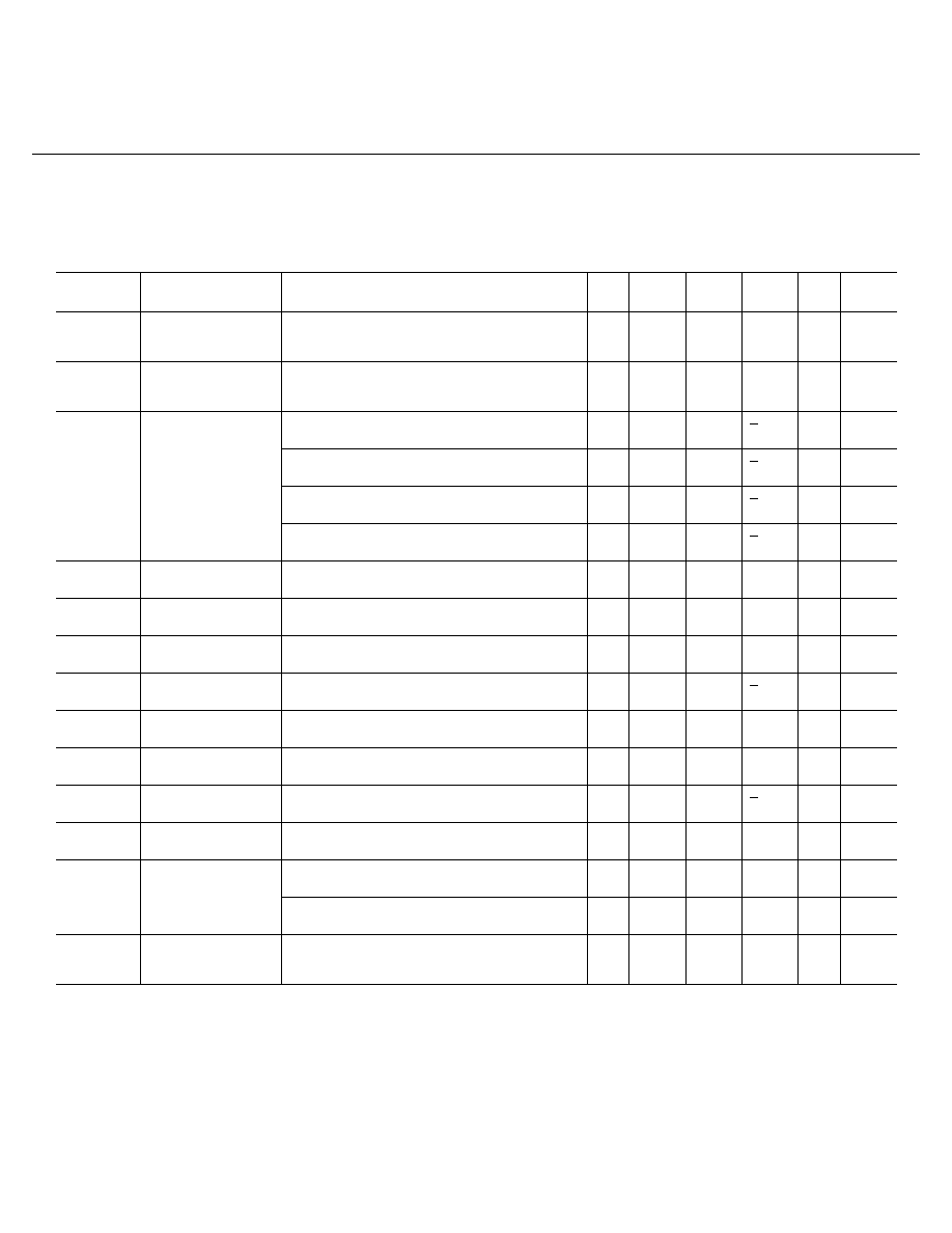
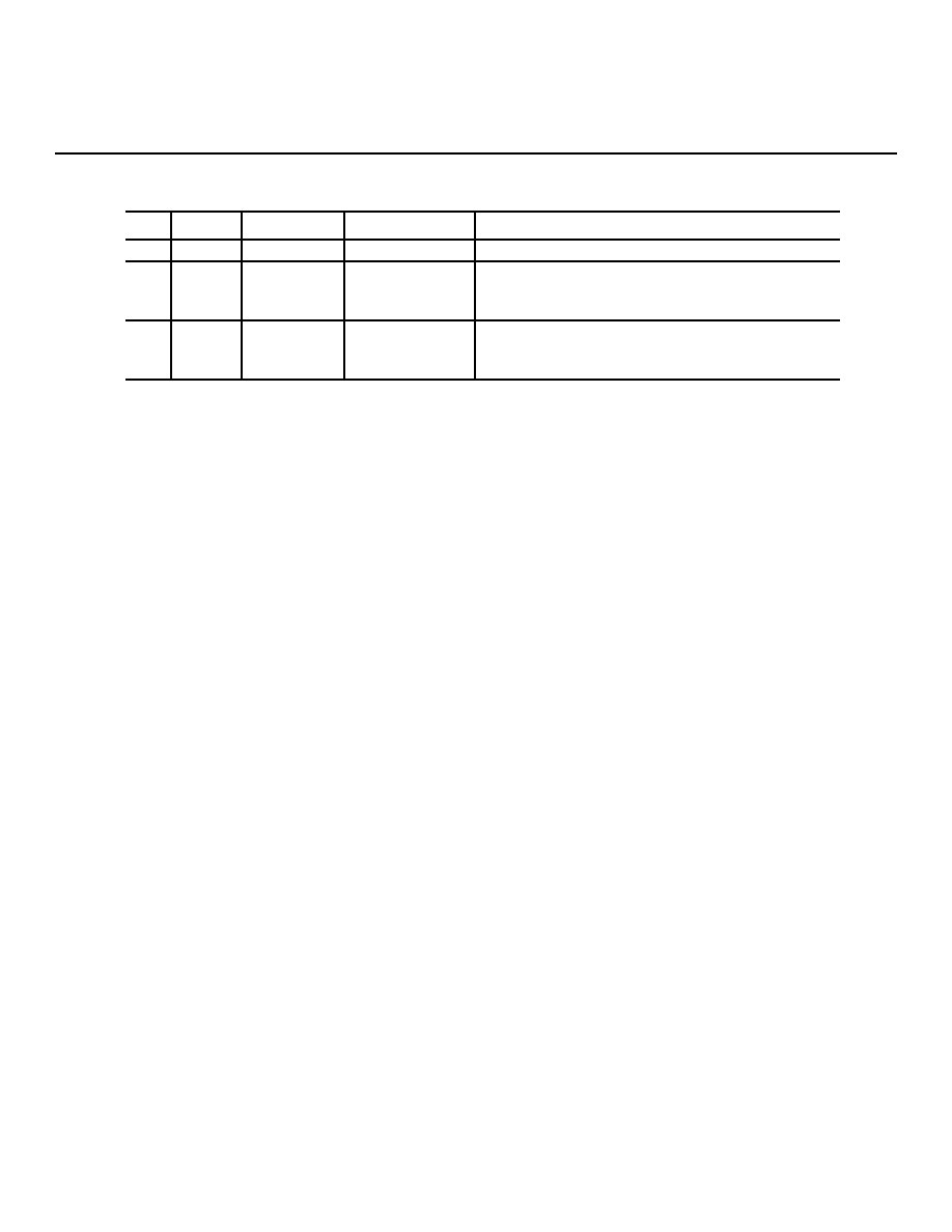
Electrical Characteristics
DC PARAMETERS: (SEE NOTE 4)
SYMBOL
PARAMETER
CONDITIONS
NOTES
PIN-
NAME
MIN
MAX
UNIT
SUB-
GROUPS
VTL
Differential
Input Low
Threshold
Vcm = +1.2V
1
RIN+,
RIN-
-100
mV
1, 2,
3
VTH
Differential
Input High
Threshold
Vcm = +1.2V
1
RIN+,
RIN-
100
mV
1, 2,
3
IIN
Input Current
Vcc=5.5V, Vin = 2.4V
RIN+,
RIN-
+10
uA
1, 2,
3
Vcc = 5.5V, Vin = 0
RIN+,
RIN-
+10
uA
1, 2,
3
Vcc = 0.0V, Vin = 2.4V
RIN+,
RIN-
+10
uA
1, 2,
3
Vcc = 0.0V, Vin = 0.0V
RIN+,
RIN-
+10
uA
1, 2,
3
VOH
Output High
Voltage
Vcc= 4.5V, Ioh = -0.4 mA, Vid = 200mV
ROUT
3.8
V
1, 2,
3
VOL
Output Low
Voltage
Vcc = 4.5, Iol = 2 mA, Vid = -200mV
ROUT
0.3
V
1, 2,
3
IOS
Output Short
Circuit Current
Enabled, Vout = 0V
ROUT
-15
-100
mA
1, 2,
3
IOZ
Output TRI-STATE
Current
Disabled, Vout = 0V or Vcc
ROUT
+10
uA
1, 2,
3
VIH
Input High
Voltage
1
EN,EN*
2.0
V
1, 2,
3
VIL
Input Low Voltage
1
EN,EN*
0.8
V
1, 2,
3
II
Input Current
VCC = 5.5V
EN, EN*
+10
uA
1, 2,
3
VCL
Input Clamp
Voltage
Icl = -18mA
EN, EN*
-1.5
V
1, 2,
3
Icc
No Load Supply
Current
EN, EN* = Vcc or GND, Inputs Open
Vcc
11
mA
1, 2,
3
EN, EN* = 2.4 or 0.5, Inputs Open
Vcc
11
mA
1, 2,
3
IccZ
No Load Supply
Current Receivers
Disabled
EN = GND, EN* = Vcc , Inputs Open
Vcc
11
mA
1, 2,
3
4
MNDS90C032-X-RH REV 1B1
MICROCIRCUIT DATA SHEET
Electrical Characteristics
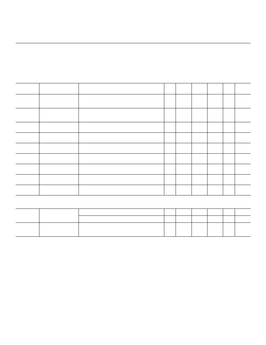
AC PARAMETERS: (SEE NOTE 4)
(The following conditions apply to all the following parameters, unless otherwise specified.)
AC:
VCC = 4.5V/5.0V/5.5V, CL = 20pF
SYMBOL
PARAMETER
CONDITIONS
NOTES
PIN-
NAME
MIN
MAX
UNIT
SUB-
GROUPS
tPHLD
Differential
Propagation Delay
High to Low
Vid = 200mV, Input pulse = 1.1V to
1.3V, Vin = 1.2V (0 differential) to
Vout = 1/2 Vcc
1.0
8
ns
9, 10,
11
tPLHD
Differential
Propagation Delay
Low to High
Vid = 200mV, Input pulse = 1.1V to
1.3V, Vin = 1.2V (0V differential) to
Vout = 1/2 Vcc
1.0
8
ns
9, 10,
11
tSKD
Differential Skew
|tPHLD-tPLHD|
CL = 20pF, Vid = 200mV
3
ns
9, 10,
11
tSK1
Channel to
Channel Skew
CL = 20pF, Vid = 200mV
2
3
ns
9, 10,
11
tSK2
Chip to Chip Skew
CL = 20pF, Vid = 200mV
3
7
ns
9, 10,
11
tPLZ
Disable Time Low
to Z
Input pulse = 0V to 3.0V, Vin = 1.5V,
Vout = Vol+0.5V, Rload = 1k Ohm to VCC
20
ns
9, 10,
11
tPHZ
Disable Time High
to Z
Input pulse = 0V to 3.0V, Vin = 1.5V,
Vout = Voh-0.5V, Rload = 1k Ohm to GND
20
ns
9, 10,
11
tPZH
Enable Time Z to
High
Input pulse = 0V to 3.0V, Vin = 1.5V,
Vout = 50%, Rload = 1k Ohm to GND
20
ns
9, 10,
11
tPZL
Enable Time Z to
Low
Input pulse = 0V to 3.0V, Vin = 1.5V,
Vout = 50%, Rload = 1k Ohm to VCC
20
ns
9, 10,
11
AC/DC PARAMETERS: POST RADIATION LIMITS (SEE NOTE 4)
Icc
No Load Supply
Current
EN, EN* = Vcc or GND, Inputs Open
20
mA
1
EN, EN* = 2.4 or 0.5, Inputs Open
20
mA
1
Iccz
No Load Supply
Current Receivers
Disabled
EN = GND, EN* = Vcc, Inputs Open
20
mA
1
Note 1:
Tested during VOH/VOL tests.
Note 2:
Channel to Channel Skew is defined as the difference between the propagation delay of
one channel and that of the others on the same chip with an event on the inputs.
Note 3:
Chip to Chip Skew is defined as the difference between the minimum and maximum
specified differential propagation delays.
Note 4:
Pre and post irradiaton limits are identical to those listed under AC and DC
electrical characteristics except as listed in the Post Radiation Limits Table (IF
APPLICABLE). Radiation end point limits for the noted parameters are guaranteed only
for the conditions as specified.
5
MICROCIRCUIT DATA SHEET
MNDS90C032-X-RH REV 1B1
Graphics and Diagrams
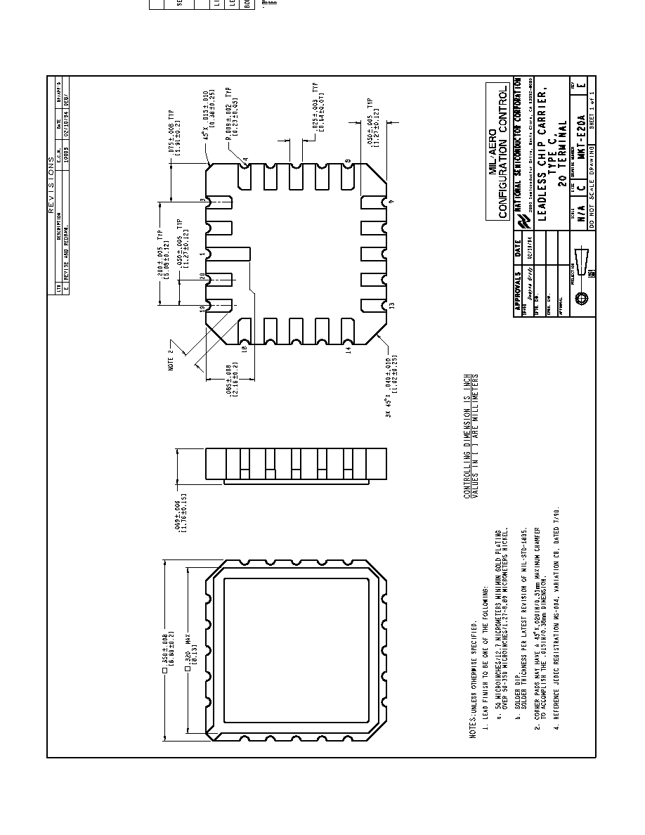
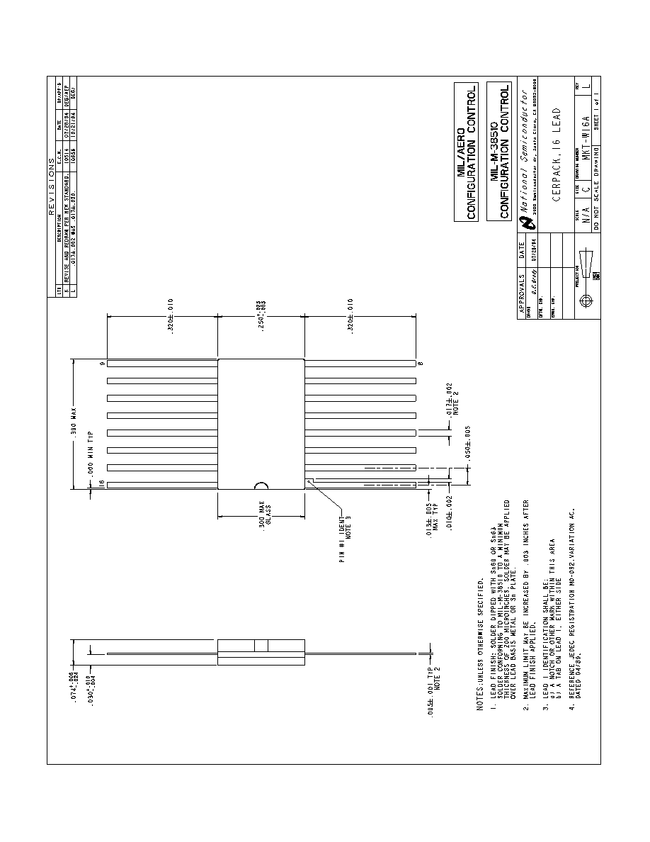
GRAPHICS#
DESCRIPTION
E20ARE
LCC (E), TYPE C, 20 TERMINAL(P/P DWG)
W16ARL
CERPACK (W), 16 LEAD (P/P DWG)
WG16ARC
CERAMIC SOIC (WG), 16 LEAD (P/P DWG)
See attached graphics following this page.
6
MICROCIRCUIT DATA SHEET
MNDS90C032-X-RH REV 1B1
Revision History
Rev
ECN #
Rel Date
Originator
Changes
0A0
M0003844
06/21/02
Rose Malone
Initial MDS Release
1A1
M0004012
08/15/03
Rose Malone
Update MDS: MNDS90C032-X-RH, Rev. 0A0 to
MNDS90C032-X-RH, Rev. 1A1. Added reference to WG pkg
to Main Table, Features Section, Absolute Maximum
Section and Graphics Section.
1B1
M0004182
08/15/03
Rose Malone
Update MDS: MNDS90C032-X-RH, Rev. 1A1 to 1B1. MDS
enhancements: Additional verbage to the general
discription, Main Table and Added new bullet to the
Features Section.
7