TL D 11367
NM27P040
4194304-Bit
(512K
x
8
)
Processor
Oriented
CMOS
EPROM
December 1993
NM27P040
4 194 304-Bit (512K x 8) Processor Oriented
CMOS EPROM
General Description
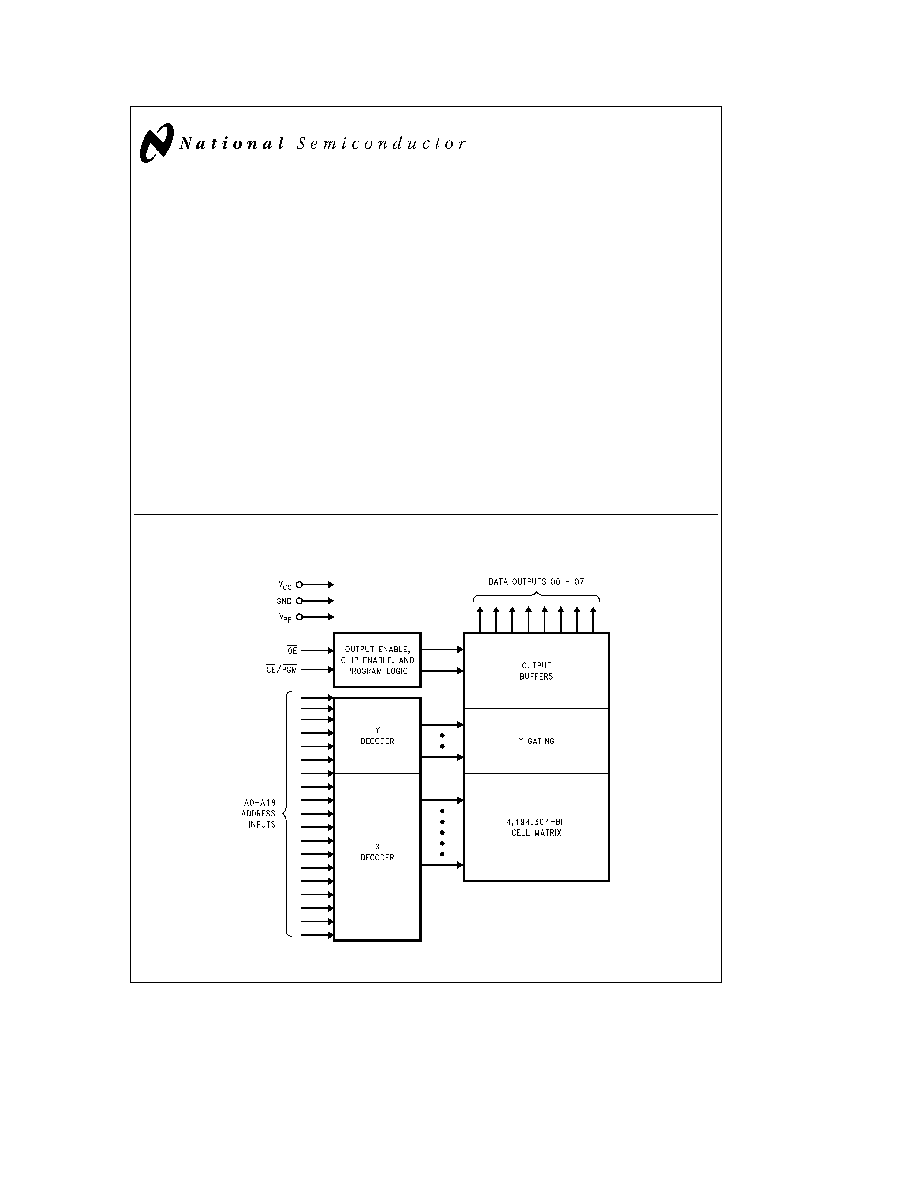
The NM27P040 is a 4096K Processor Oriented EPROM
(POP
TM
) configured as 512K x 8 It's designed to simplify
microprocessor interfacing while remaining compatible with
standard EPROMs It can reduce both wait states and glue
logic when the specification improvements are taken advan-
tage of in the system design The NM27P040 is implement-
ed in National's advanced CMOS EPROM process to pro-
vide a reliable solution and access times as fast as 120 ns
The interface improvements address two areas to eliminate
the need for additional devices to adapt the EPROM to the
microprocessor and to eliminate wait states at the termina-
tion of the access cycle Even with these improvements the
NM27P040 remains compatible with industry standard
JEDEC pinout EPROMs The time from CE or OE being
negated until the outputs are guaranteed to be in the high
impedance state has been reduced to eliminate the need
for wait states at the termination of the memory cycle and
the data-out hold time has been extended to eliminate the
need to provide data hold time for the microprocessor by
delaying control signals or latching and holding the data in
external latches
Features
Y
Fast output turn off to eliminate wait states
Y
Extended data hold time for microprocessor
compatibility
Y
High performance CMOS
120 ns access time
Y
JEDEC standard pin configuration
Y
Manufacturer's identification code
Block Diagram
TL D 11367 ≠ 1
TRI-STATE
is a registered trademark of National Semiconductor Corporation
POP
TM
is a trademark of National Semiconductor Corporation
C1995 National Semiconductor Corporation
RRD-B30M105 Printed in U S A

Connection Diagrams
27C080
27C020
27C010
A19
XX V
PP
XX V
PP
A16
A16
A16
A15
A15
A15
A12
A12
A12
A7
A7
A7
A6
A6
A6
A5
A5
A5
A4
A4
A4
A3
A3
A3
A2
A2
A2
A1
A1
A1
A0
A0
A0
O
0
O
0
O
0
O
1
O
1
O
1
O
2
O
2
O
2
GND
GND
GND
DIP
NM27P040
TL D 11367 ≠ 2
27C010
27C020
27C080
V
CC
V
CC
V
CC
XX PGM
XX PGM
A18
XX
A17
A17
A14
A14
A14
A13
A13
A13
A8
A8
A8
A9
A9
A9
A11
A11
A11
OE
OE
OE V
PP
A10
A10
A10
CE
CE
CE PGM
O
7
O
7
O
7
O
6
O
6
O
6
O
5
O
5
O
5
O
4
O
4
O
4
O
3
O
3
O
3
Note
Compatible EPROM pin configurations are shown in the blocks adjacent to the NM27P040 pin
Commercial Temperature Range (0 C to
a
70 C)
V
CC
e
5V
g
10%
Parameter Order Number
Access Time (ns)
NM27P040 Q 120
120
NM27P040 Q 150
150
NM27P040 Q 170
170
Extended Temperature Range (
b
40 C to
a
85 C)
V
CC
e
5V
g
10%
Parameter Order Number
Access Time (ns)
NM27P040 QE 150
150
NM27P040 QE 170
170
Military Temperature Range (
b
55 C to
a
125 C)
V
CC
e
5V
g
10%
Parameter Order Number
Access Time (ns)
NM27P040 QM 150
150
NM27P040 QM 200
200
Package Types NM27P040 QXXX
Q
e
Quartz-Windowed Ceramic DIP
All packages conform to the JEDEC standard
All versions are guaranteed to function for slower
speeds
Pin Names
A0 ≠ A18
Addresses
CE PGM
Chip Enable Program
OE
Output Enable
O0 ≠ O7
Outputs
XX
Don't Care (During Read)
2
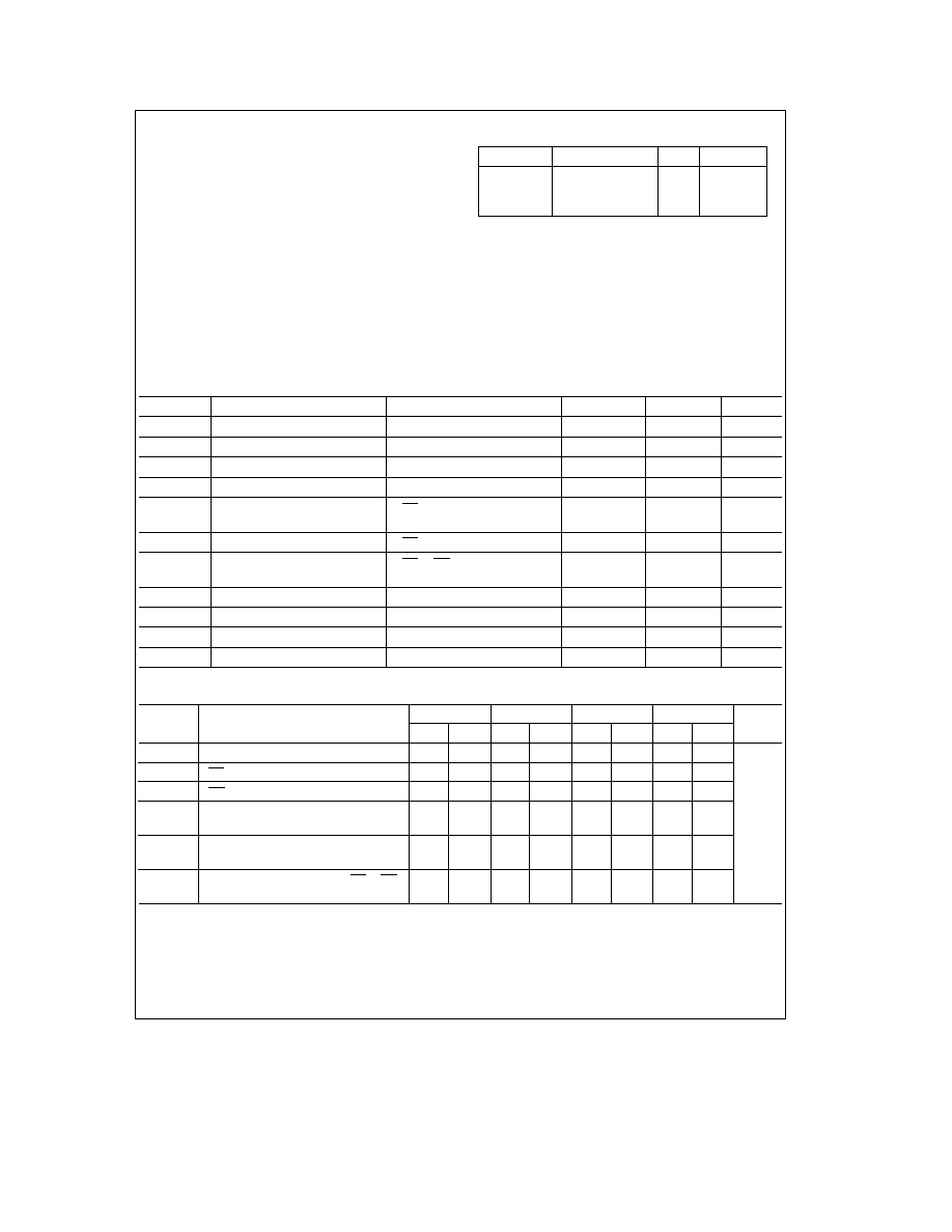
Absolute Maximum Ratings
(Note 1)
If Military Aerospace specified devices are required
please contact the National Semiconductor Sales
Office Distributors for availability and specifications
Storage Temperature
b
65 C to
a
150 C
All Input Voltages except A9 with
Respect to Ground (Note 10)
b
0 6V to
a
7V
V
PP
and A9 with Respect to Ground
b
0 6V to
a
14V
V
CC
Supply Voltage with
Respect to Ground
b
0 6V to
a
7V
ESD Protection
l
2000V
All Output Voltages with
Respect to Ground (Note 10) V
CC
a
1 0V to GND
b
0 6V
Operating Range
Range
Temperature
V
CC
Tolerance
Commercial
0 C to
a
70 C
a
5V
g
10%
Industrial
b
40 C to
a
85 C
g
5V
g
10%
Military
b
55 C to
a
125 C
g
5V
g
10%
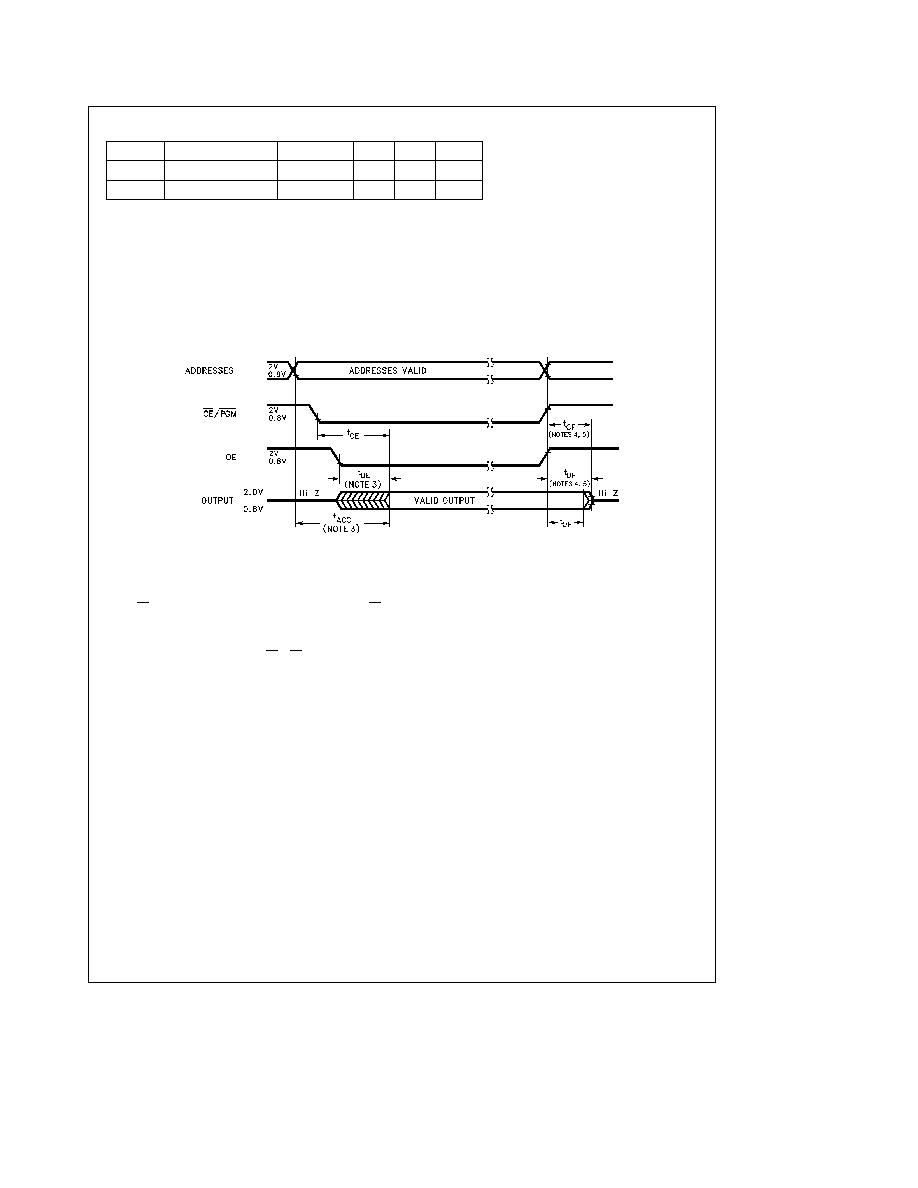
Read Operation
DC Electrical Characteristics
Over operating range with V
PP
e
V
CC
Symbol
Parameter
Test Conditions
Min
Max
Units
V
IL
Input Low Level
b
0 2
0 8
V
V
IH
Input High Level
2 0
V
CC
a
1
V
V
OL
Output Low Voltage
I
OL
e
2 1 mA
0 4
V
V
OH
Output High Voltage
I
OH
e b
2 5 mA
3 5
V
I
SB1
V
CC
Standby Current (CMOS)
CE
e
V
CC
g
0 3V
100
m
A
(Note 11)
I
SB2
V
CC
Standby Current
CE
e
V
IH
1
mA
I
CC
V
CC
Active Current
CE
e
OE
e
V
IL
I O
e
0 mA
30
mA
f
e
5 MHz
I
PP
V
PP
Supply Current
V
PP
e
V
CC
10
m
A
V
PP
V
PP
Read Voltage
V
CC
b
0 4
V
CC
V
I
LI
Input Load Current
V
IN
e
5 5V or GND
b
1
1
m
A
I
LO
Output Leakage Current
V
OUT
e
5 5V or GND
b
10
10
m
A
AC Electrical Characteristics
Over operating range with V
PP
e
V
CC
Symbol
Parameter
120
150
170
250
Units
Min
Max
Min
Max
Min
Max
Min
Max
t
ACC
Address to Output Delay
120
150
170
250
ns
t
CE
CE to Output Delay
120
150
170
250
t
OE
OE to Output Delay
50
50
50
50
t
DF
Output Disable to
35
25
25
25
(Note 2)
Output Float
t
CF
Chip Disable to
35
30
30
30
(Note 2)
Output Float
t
OH
Output Hold from Addresses CE or OE
7
7
7
7
(Note 2)
Whichever Occurred First
3
Capacitance
T
A
e a
25 C f
e
1 MHz (Note 2)
Symbol
Parameter
Conditions
Typ
Max
Units
C
IN
Input Capacitance
V
IN
e
0V
9
15
pF
C
OUT
Output Capacitance
V
OUT
e
0V
12
15
pF
AC Test Conditions
Output Load
1 TTL Gate and
C
L
e
100 pF (Note 8)
Input Rise and Fall Times
s
5 ns
Input Pulse Levels
0 45V to 2 4V
Timing Measurement Reference Level
Inputs
0 8V and 2V
Outputs
0 8V and 2V
AC Waveforms
(Notes 6 7 and 9)
TL D 11367 ≠ 3
Note 1
Stresses above those listed under ``Absolute Maximum Ratings'' may cause permanent damage to the device This is a stress rating only and functional
operation of the device at these or any other conditions above those indicated in the operational sections of this specification is not implied Exposure to absolute
maximum rating conditions for extended periods may affect device reliability
Note 2
This parameter is only sampled and is not 100% tested
Note 3
OE may be delayed up to t
ACC
b
t
OE
after the falling edge of CE without impacting t
ACC
Note 4
The t
DF
and t
CF
compare level is determined as follows
High to TRI-STATE
the measured V
OH1
(DC)
b
0 10V
Low to TRI-STATE the measured V
OL1
(DC)
a
0 10V
Note 5
TRI-STATE may be attained using OE or CE
Note 6
The power switching characteristics of EPROMs require careful device decoupling It is recommended that at least a 0 1 mF ceramic capacitor be used on
every device between V
CC
and GND
Note 7
The outputs must be restricted to V
CC
a
1 0V to avoid latch-up and device damage
Note 8
1 TTL Gate I
OL
e
1 6 mA I
OH
e b
400 mA
C
L
100 pF includes fixture capacitance
Note 9
V
PP
may be connected to V
CC
except during programming
Note 10
Inputs and outputs can undershoot to
b
2 0V for 20 ns Max
Note 11
CMOS input V
IL
e
GND
g
0 3V V
IH
e
V
CC
g
0 3V
4

Programming Waveform
(Note 3)
TL D 11367 ≠ 4
5