 | –≠–ª–µ–∫—Ç—Ä–æ–Ω–Ω—ã–π –∫–æ–º–ø–æ–Ω–µ–Ω—Ç: NM27P512 | –°–∫–∞—á–∞—Ç—å:  PDF PDF  ZIP ZIP |
TL D 11365
NM27P512
524288-Bit
(64K
x
8
)
Processor
Oriented
CMOS
EPROM
December 1993
NM27P512
524 288-Bit (64K x 8) Processor Oriented
CMOS EPROM
General Description
The NM27P512 is a 512K Processor Oriented EPROM con-
figured as 64k x 8 It's designed to simplify microprocessor
interfacing while remaining compatible with standard
EPROMs It can reduce both wait states and glue logic
when the specification improvements are taken advantage
of in the system design The NM27P512 is implemented in
National's advanced CMOS EPROM process to provide ex-
cellent reliability and access times as fast as 120 ns
The interface improvements address two areas to eliminate
the need for additional devices to adapt the EPROM to the
microprocessor and to eliminate wait states at the termina-
tion of the access cycle Even with these improvements the
NM27P512 remains compatible with industry standard
JEDEC pinout EPROMs The maximum specification for out-
put turn-off time has been reduced eliminating the need for
wait states at the end of a read cycle Also the minimum
specification for output hold time has been increased elimi-
nating the need for external circuitry to hold the data
Features
Y
Fast output turn off to eliminate wait states
Y
Extended data hold time for microprocessor
compatibility
Y
High performance CMOS
120 ns access time
Y
JEDEC standard pin configuration
Y
Manufacturer's identification code
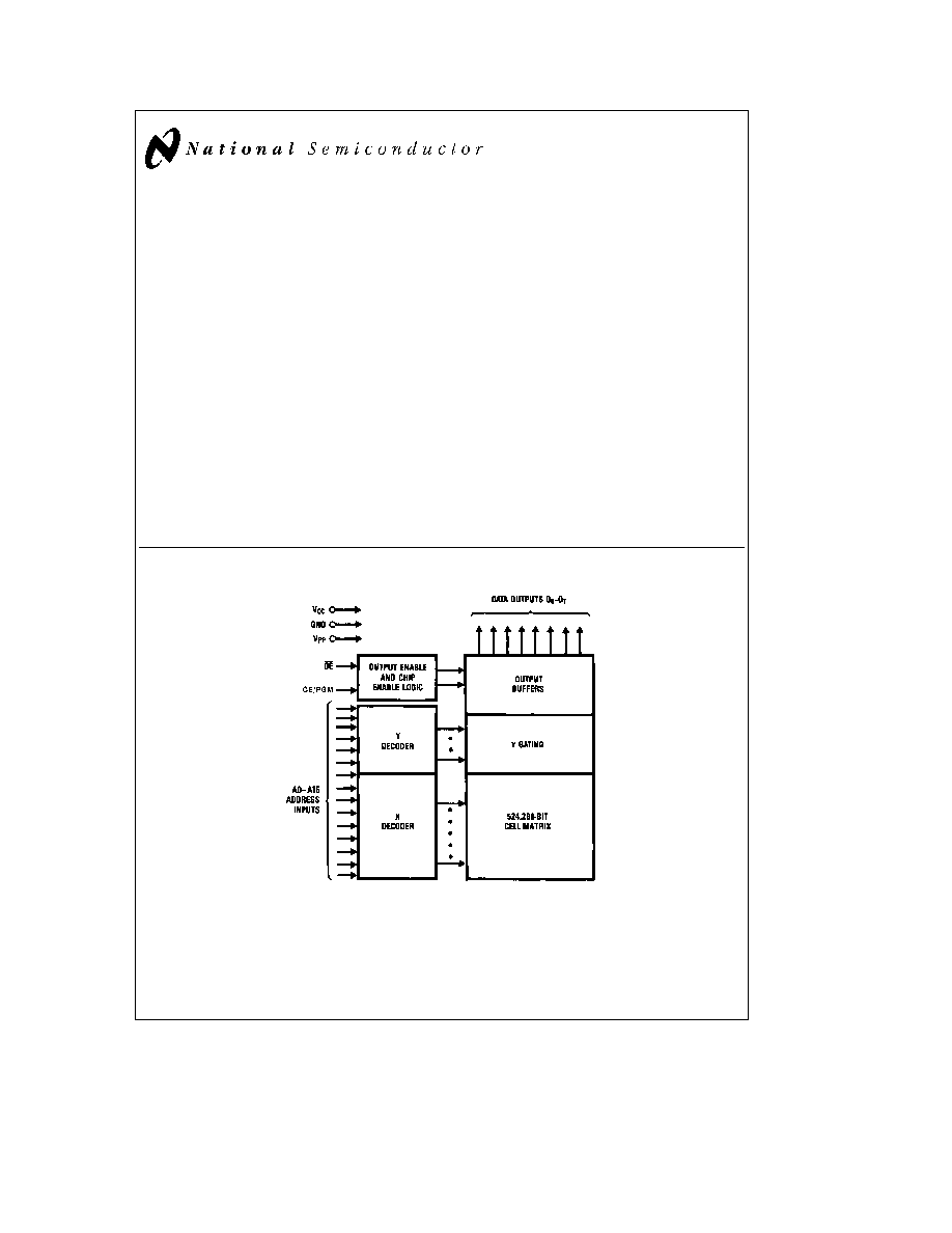
Block Diagram
TL D 11365 ≠ 1
TRI-STATE
is a registered trademark of National Semiconductor Corporation
NSC800
TM
is a trademark of National Semiconductor Corporation
C1995 National Semiconductor Corporation
RRD-B30M105 Printed in U S A
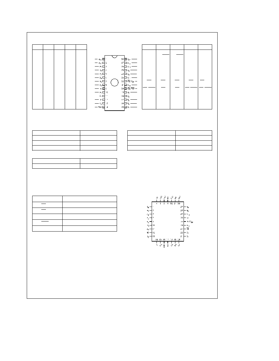
Connection Diagrams
27C080 27C040 27C020 27C010 27C256
A
19
XX V
PP
XX V
PP
XX V
PP
A
16
A
16
A
16
A
16
A
15
A
15
A
15
A
15
V
PP
A
12
A
12
A
12
A
12
A
12
A
7
A
7
A
7
A
7
A
7
A
6
A
6
A
6
A
6
A
6
A
5
A
5
A
5
A
5
A
5
A
4
A
4
A
4
A
4
A
4
A
3
A
3
A
3
A
3
A
3
A
2
A
2
A
2
A
2
A
2
A
1
A
1
A
1
A
1
A
1
A
0
A
0
A
0
A
0
A
0
O
0
O
0
O
0
O
0
O
0
O
1
O
1
O
1
O
1
O
1
O
2
O
2
O
2
O
2
O
2
GND
GND
GND
GND
GND
DIP
NM27P512
TL D 11365 ≠ 2
27C256
27C010
27C020
27C040
27C080
V
CC
V
CC
V
CC
V
CC
XX PGM XX PGM
A
18
A
18
V
CC
XX
A
17
A
17
A
17
A
14
A
14
A
14
A
14
A
14
A
13
A
13
A
13
A
13
A
13
A
8
A
8
A
8
A
8
A
8
A
9
A
9
A
9
A
9
A
9
A
11
A
11
A
11
A
11
A
11
OE
OE
OE
OE
OE
VPP
A
10
A
10
A
10
A
10
A
10
CE PGM
CE
CE
CE PGM CE PGM
O
7
O
7
O
7
O
7
O
7
O
6
O
6
O
6
O
6
O
6
O
5
O
5
O
5
O
5
O
5
O
4
O
4
O
4
O
4
O
4
O
3
O
3
O
3
O
3
O
3
Note
Compatible EPROM pin configurations are shown in the blocks adjacent to the NM27P512 pins
Commercial Temp Range (0 C to
a
70 C)
Parameter Order Number
Access Time (ns)
NM27P512 Q N V 120
120
NM27P512 Q N V 150
150
NM27P512 Q N V 200
200
Military Temp Range (
b
55 C to
a
125 C)
Parameter Order Number
Access Time (ns)
NM27P512 QM 200
200
Extended Temp Range (
b
40 C to
a
85 C)
Parameter Order Number
Access Time (ns)
NM27P512 QE NE VE 120
120
NM27P512 QE NE VE 150
150
NM27P512 QE NE VE 200
200
Note
Surface mount PLCC package available for commercial and extended
temperature ranges only
All versions are guaranteed to function for slower speeds
Package Types NM27P512 Q N V XXX
Q
e
Quartz-Windowed Ceramic DIP Package
N
e
Plastic OTP DIP Package
V
e
PLCC Package
All packages conform to the JEDEC standard
Pin Names
A0 ≠ A15
Addresses
CE
Chip Enable
OE
Output Enable
O0 ≠ O7
Outputs
PGM
Program
XX
Don't Care (During Read)
PLCC
TL D 11365 ≠ 3
2
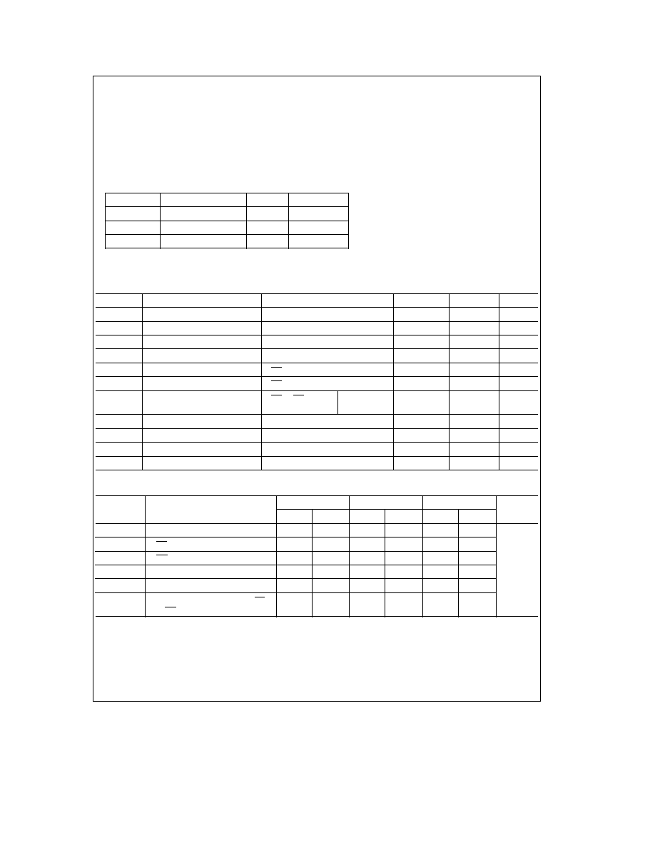
Absolute Maximum Ratings
(Note 1)
If Military Aerospace specified devices are required
please contact the National Semiconductor Sales
Office Distributors for availability and specifications
Storage Temperature
b
65 C to
a
150 C
All Input Voltages Except A9 with
Respect to Ground
b
0 6V to
a
7V
V
PP
and A9 with Respect to Ground
b
0 7V to
a
14V
V
CC
Supply Voltage with
Respect to Ground
b
0 6V to
a
7V
ESD Protection
(MIL Std 883 Method 3015 2)
l
2000V
All Output Voltages with
Respect to Ground
V
CC
a
1 0V to GND
b
0 6V
Operating Range
Range
Temperature
V
CC
Tolerance
Comm'l
0 C to
a
70 C
a
5V
g
10%
Industrial
b
40 C to
a
85 C
a
5V
g
10%
Military
b
55 C to
a
125 C
a
5V
g
10%
Read Operation
DC Electrical Characteristics
Symbol
Parameter
Test Conditions
Min
Max
Units
V
IL
Input Low Level
b
0 5
08
V
V
IH
Input High Level
2 0
V
CC
a
1
V
V
OL
Output Low Voltage
I
OL
e
2 1 mA
0 4
V
V
OH
Output High Voltage
I
OH
e b
2 5 mA
3 5
V
I
SB1
(10)
V
CC
Standby Current (CMOS)
CE
e
V
CC
g
0 3V
100
m
A
I
SB2
V
CC
Standby Current
CE
e
V
IH
1
mA
I
CC
V
CC
Active Current
CE
e
OE
e
V
IL
f
e
5 MHz
40
mA
I O
e
0 mA
I
PP
V
PP
Supply Current
V
PP
e
V
CC
10
m
A
V
PP
V
PP
Read Voltage
V
CC
b
0 7
V
CC
V
I
LI
Input Load Current
V
IN
e
5 5V or GND
b
1
1
m
A
I
LO
Output Leakage Current
V
OUT
e
5 5V or GND
b
10
10
m
A
AC Electrical Characteristics
Symbol
Parameter
120
150
200
Units
Min
Max
Min
Max
Min
Max
t
ACC
Address to Output Delay
120
150
200
ns
t
CE
CE to Output Delay
120
150
200
t
OE
OE to Output Delay
50
50
50
t
DF
(2)
Output Disable to Output Float
25
25
25
t
CF
(2)
Chip Disable to Output Float
30
30
30
t
OH
(2)
Output Hold from Addresses CE
7
7
7
or OE Whichever Occurred First
3
Capacitance
T
A
e a
25 C f
e
1 MHz (Note 2)
Symbol
Parameter
Conditions
Typ
Max
Units
C
IN1
Input Capacitance
V
IN
e
0V
6
12
pF
except OE V
PP
C
OUT
Output Capacitance
V
OUT
e
0V
9
12
pF
C
IN2
OE V
PP
Input
V
IN
e
0V
20
25
pF
Capacitance
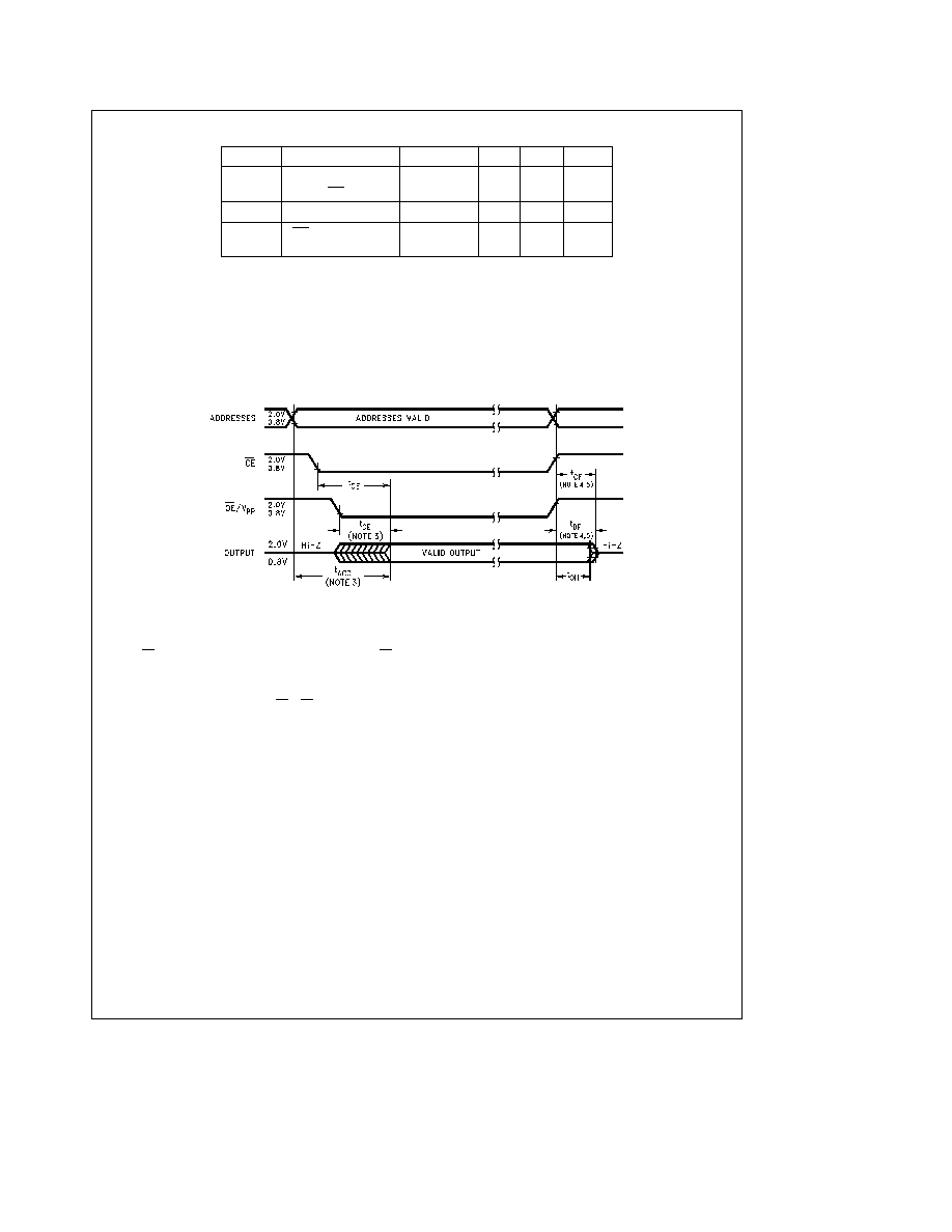
AC Test Conditions
Output Load
1 TTL Gate and
C
L
e
100 pF (Note 8)
Input Rise and Fall Times
s
5 ns
Input Pulse Levels
0 45V to 2 4V
Timing Measurement Reference Level (Note 9)
Inputs
0 8V and 2V
Outputs
0 8V and 2V
AC Waveforms
(Notes 6 7)
TL D 11365 ≠ 4
Note 1
Stresses above those listed under ``Absolute Maximum Ratings'' may cause permanent damage to the device This is a stress rating only and functional
operation of the device at these or any other conditions above those indicated in the operational sections of this specification is not implied Exposure to absolute
maximum rating conditions for extended periods may affect device reliability
Note 2
This parameter is only sampled and is not 100% tested
Note 3
OE may be delayed up to t
ACC
≠ t
OE
after the falling edge of CE without impacting t
ACC
Note 4
The t
DF
and t
CF
compare level is determined as follows
High to TRI-STATE the measured V
OH1
(DC)
b
0 10V
Low to TRI-STATE the measured V
OL1
(DC)
a
0 10V
Note 5
TRI-STATE may be attained using OE or CE
Note 6
The power switching characteristics of EPROMs require careful device decoupling It is recommended that at least a 0 1 mF ceramic capacitor be used on
every device between V
CC
and GND
Note 7
The outputs must be restricted to V
CC
a
1 0V to avoid latch-up and device damage
Note 8
1 TTL Gate I
OL
e
1 6 mA I
OH
e b
400 mA
C
L
100 pF includes fixture capacitance
Note 9
Inputs and outputs can undershoot to
b
2 0V for 20 ns Max
Note 10
CMOS inputs V
IL
e
GND
g
0 3V V
IH
e
V
CC
g
0 3V
4
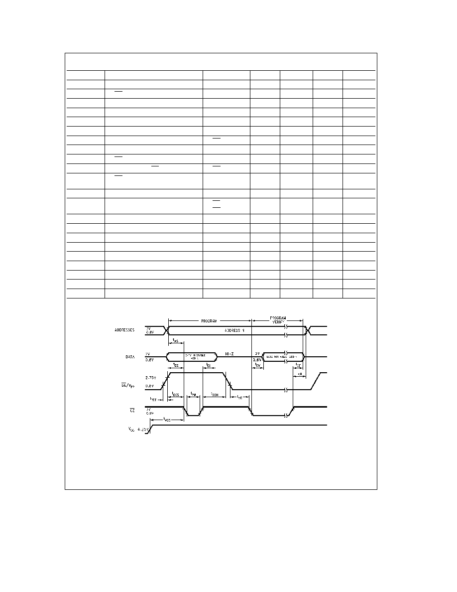
Programming Characteristics
(Notes 1 and 2)
Symbol
Parameter
Conditions
Min
Typ
Max
Units
t
AS
Address Setup Time
1
m
s
t
OES
OE Setup Time
1
m
s
t
DS
Data Setup Time
1
m
s
t
VCS
V
CC
Setup Time
1
m
s
t
AH
Address Hold Time
0
m
s
t
DH
Data Hold Time
1
m
s
t
CF
Chip Enable to Output Float Delay
OE
e
V
IL
0
60
ns
t
PW
Program Pulse Width
95
100
105
m
s
t
OEH
OE Hold Time
1
m
s
t
DV
Data Valid from CE
OE
e
V
IL
250
ns
t
PRT
OE Pulse Rise Time
50
ns
during Programming
t
VR
V
PP
Recovery Time
1
m
s
I
PP
V
PP
Supply Current during
CE
e
V
IL
30
mA
Programming Pulse
OE
e
V
PP
I
CC
V
CC
Supply Current
50
mA
T
R
Temperature Ambient
20
25
30
C
V
CC
Power Supply Voltage
6
6 25
6 5
V
V
PP
Programming Supply Voltage
12 5
12 75
13
V
t
FR
Input Rise Fall Time
5
ns
V
IL
Input Low Voltage
0
0 45
V
V
IH
Input High Voltage
2 4
4
V
t
IN
Input Timing Reference Voltage
0 8
2
V
t
OUT
Output Timing Reference Voltage
0 8
2
V
Programming Waveforms
TL D 11365 ≠ 5
Note 1
National's standard product warranty applies to devices programmed to specifications described herein
Note 2
V
CC
must be applied simultaneously or before V
PP
and removed simultaneously or after V
PP
The EPROM must not be inserted into or removed from a
board with voltage applied to V
PP
or V
CC
Note 3
The maximum absolute allowable voltage which may be applied to the V
PP
pin during programming is 14V Care must be taken when switching the V
PP
supply to prevent any overshoot from exceeding this 14V maximum specification At least a 0 1 mF capacitor is required across V
CC
to GND to suppress spurious
voltage transients which may damage the device
Note 4
Programming and program verify are tested with the fast Program Algorithm at typical power supply voltages and timings
5