 | –≠–ª–µ–∫—Ç—Ä–æ–Ω–Ω—ã–π –∫–æ–º–ø–æ–Ω–µ–Ω—Ç: NM29A080V | –°–∫–∞—á–∞—Ç—å:  PDF PDF  ZIP ZIP |
TL D 12475
NM29A040080
4-Mbit8-Mbit
CMOS
Serial
FLASH
E
2
PROM
February 1996
NM29A040 080
4-Mbit 8-Mbit CMOS Serial FLASH E
2
PROM
General Description
The NM29A040 080 are 4-Mbit and 8-Mbit Flash memories
designed with a MICROWIRE
TM
serial interface All of the
features of the device are designed to provide the most cost
effective solution for applications requiring low bandwidth
file storage Examples of these applications include digital
answering machines and personal digital recorders (digital
audio) or FAX and digital scanners (digital imaging) The
Serial Flash requires only a single 5V power supply has a
small erase block size (4 kbytes) and a low EMI serial inter-
face
The NM29A040 080 have been designed to work seam-
lessly
with
National's
CompactRISC
TM
family
(e g
NSAM266) of processors In this manner National is able to
provide the complete system solution to digital audio re-
cording (processor CODEC Flash memory software) or
digital imaging
Features
Y
Single 5V
g
10% power supply
Y
4 kbyte erase block
Y
Organized as 128 (256) Blocks per 4-Mbit (8-Mbit)
Device
128 pages per block
32 bytes per page (256 bits)
Y
MICROWIRE
TM
compatible interface
Y
Low operating current (typical)
5 mA read current
15 mA write current
10 mA erase current
5 mA standby current
Y
100k write erase cycle endurance
Y
Offered in PLCC and SOIC packages
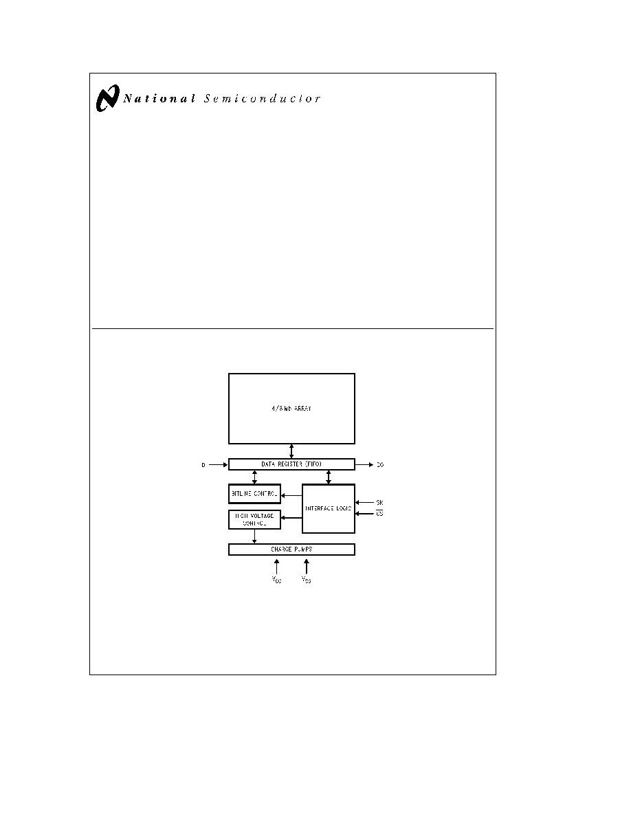
Block Diagram
TL D 12475 ≠ 1
TRI-STATE
is a registered trademark of National Semiconductor Corporation
MICROWIRE
TM
SpeechPro
TM
CompactRISC
TM
and CompactSPEECH
TM
are trademarks of National Semiconductor Corporation
C1996 National Semiconductor Corporation
RRD-B30M36 Printed in U S A
http
www national com
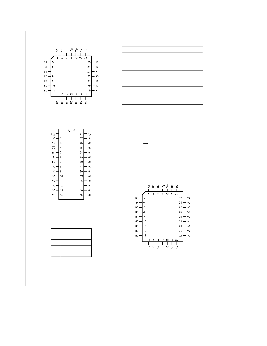
Connection Diagrams
Plastic Chip Carrier (V)
TL D 12475 ≠ 2
NM29A040V
NS Package Number V28A
Small Outline Package (M)
TL D 12475 ≠ 3
NM29A040M
NM29A080M
NS Package Number MA28A
Pin Assignments
DO
Serial Data Output
DI
Serial Data Input
SK
Serial Data Clock
CS
Chip Select
NC
No Connection
Ordering Information
Commercial Temperature Range (0 C to
a
70 C)
Order Number
NM29A040V
NM29A040M
NM29A080V
NM29A080M
Extended Temp Range (
b
40 C to
a
85 C)
Order Number
NM29A040EV
NM29A040EM
NM29A080EV
NM29A080EM
Pin Functions
SERIAL DATA INPUT DI
The DI pin is used for transferring in commands and data
Data is latched on the rising edge of SK
SERIAL DATA OUT DO
The DO pin is used for transferring out status and data Data
output will change following the falling edge of SK
CHIP SELECT CS
This signal indicates which device is selected When this
signal is inactive the device ignores SK This signal can be
tied to ground when there is only one Serial Flash device
The CS pin may be pulled high to reset command input
SERIAL DATA CLOCK SK
This is the standard synchronous MICROWIRE clock which
determines the rate of data transfer On each toggle one
data bit is shifted into or out of the Serial Flash
TL D 12475 ≠ 22
NM29A080V
NS Package Number VA32A
http
www national com
2
System Concepts
The NM29A040 080 are 4-Mbit and 8-Mbit NAND Flash de-
signed to provide the most cost effective solution for file
storage applications These applications include digital au-
dio recording digital image storage and data logging appli-
cations
For digital audio storage the NM29A040 080 have been
matched with National's NSAM266 voice processor Appli-
cations that can benefit from this combination include digital
answering machines personal digital recorders pagers and
voicemail systems When combined with National Semicon-
ductor's CompactSPEECH
TM
embedded software and the
NSAM266 processor customers can quickly bring to market
systems capable of recording up to 15 minutes of audio on
a single 4 Mb device Multiple NM29A040 080's can be
used to extend the record time up to 2 hours
Digital imaging applications include FAX machines hand-
held
scanners
and
digital
cameras
Combining
the
NM29A040 080 with the CompactRISC family of embedded
processors can enable complete solutions for image stor-
age
Data logging applications can take advantage of the
NM29A040 080's simple interface and nonvolatility to allow
simple 8-bit microcontroller based systems to have access
to over 4 Mb of storage The nonvolatility ensures data in-
tegrity in remote battery powered applications
TL D 12475 ≠ 4
FIGURE 1 Digital Audio Recording Solution
TABLE I Data Transfer Rates
Transfer Rates
Total Time
Page
Block
Page
Block
Read
1 02 Mbits s
2 61 Mbits s
251 ms
12 6 ms
(127 5 kbytes s)
(325 8 kbytes s)
Write
406 3 kbits s
536 4 kbits s
630 ms
61 1 ms
(50 8 kbytes s)
(67 1 kbytes s)
Erase
6 ms
http
www national com
3

Device Operation
The basic functions required for storing messages or im-
ages on the NM29A040 080 are Page Read Page Write
and Block Erase These functions can be implemented by
combining the different instructions for the NM29A040 080
in the following sequences
PAGE READ
Page Read will read out the 32 bytes of a page for the
specified address To continue reading the page at the next
address an Increment command (90H) can be issued In
this way the system can avoid repeatedly using the three
byte Set-Address command The Increment command is
then followed by the Read command and proceeds in the
same manner as shown in
Figure 2
TL D 12475 ≠ 5
FIGURE 2 Page Read Sequence
PAGE WRITE
Page Write sequence will write up to 32 bytes into a speci-
fied page Like the Page Read sequence the Increment
command can be used to quickly set the address to the next
page for writing data sequentially into a block
TL D 12475 ≠ 6
FIGURE 3 Page Write Sequence
http
www national com
4
Device Operation
(Continued)
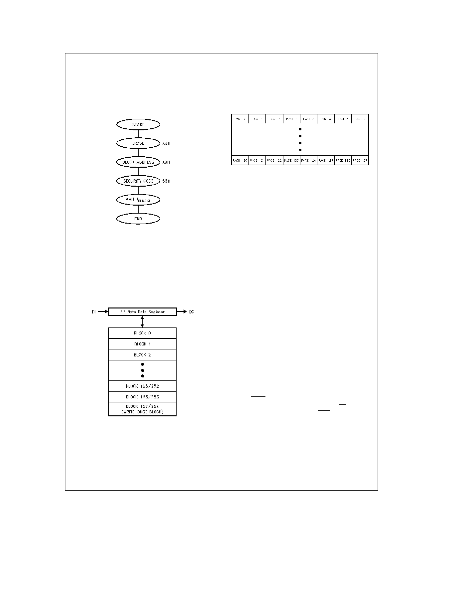
BLOCK ERASE
The Block Erase sequence erases a specified block (4 kB)
of data Flash memory devices require that a block be in an
erased state prior to writing to a memory cell In this man-
ner a block must be erased prior to the recording of any
messages or storage of any images
TL D 12475 ≠ 7
FIGURE 4 Block Erase Sequence
Functional Description
ORGANIZATION
The NM29A040 080 are 4-Mbit and 8-Mbit devices respec-
tively organized as 128 256 blocks of 128 pages A block is
the smallest unit that can be erased and is 4 kbytes in size
Within a block are 16 rows of 8 pages each row 256 bytes
long Each page is 32 bytes long Read and write operations
always operate on a page at a time
TL D 12475 ≠ 8
FIGURE 5 Device Organization
Reading or writing data to the Serial Flash involves clocking
data into or out of the data register The data register is a
32-byte wide shift register equivalent in size to one page
When shifting in a full page writing to the array and then
reading out the same page the first bit shifted in will be the
first bit shifted out If for example only 5 bytes are shifted in
written to the array and then the same page is read out 27
bytes should be shifted out before the original 5 bytes will
be shifted out See Note 4 in the notifications section for an
explanation of multiple page writes and masking
TL D 12475 ≠ 9
FIGURE 6 Block Organization
WRITE ONCE BLOCK
The NM29A040 contains 127 blocks (blocks 0 thru block
126) which are fully accessible to the user for reading writ-
ing and erasing The final block number 127 has been set
aslde as a write once block The pages in this block may
only be written to once Once the data is written it may not
be erased In this manner block 127 may be used for stor-
ing system configuration information that cannot be lost
The NM29A080 operates in a similar manner but has 253
blocks that are fully accessible Block 254 contains the un-
usable block information although this block has 256 pages
as opposed to the standard 128 pages
The last block is not accessible through the normal Read
and Write commands Special commands for Read (D0H)
and Write (F0H) are used to perform the last block opera-
tions An erase operation is not available or usable on the
last block
DATA REGISTER
The data register is a 32-byte FIFO that is used to shift data
into or out of the device When a write operation is per-
formed all 32 bytes are written to the currently addressed
page Refer to Note 4 for how to write less than 32 bytes to
a page
The data register may be used as an on-chip holding area
for partial page data For example if data is acquired exter-
nally in 8-byte multiples the data register can be used to
hold each 8-byte segment After the 4th such data segment
an entire page of data will have been accumulated at which
point the write command mat be issued No data may be
shifted into or out of the data register while the device is
busy
READY BUSY OUTPUT
When the Serial Flash device is selected with CS held low
then the DO pin reflects the Ready Busy state of the de-
vice This is true at all times except when reading data out
of the device as in the Get-Status command or the Data-
Shift-Out command When the device is unselected the DO
output is in a high impedance state
http
www national com
5