 | –≠–ª–µ–∫—Ç—Ä–æ–Ω–Ω—ã–π –∫–æ–º–ø–æ–Ω–µ–Ω—Ç: NM29N16 | –°–∫–∞—á–∞—Ç—å:  PDF PDF  ZIP ZIP |
TL D 11915
NM29N16
16
MBit
(2
M
x
8
Bit)
CMOS
NAND
FLASH
E
2
PROM
February 1996
NM29N16
16 MBit (2M x 8 Bit) CMOS NAND FLASH E
2
PROM
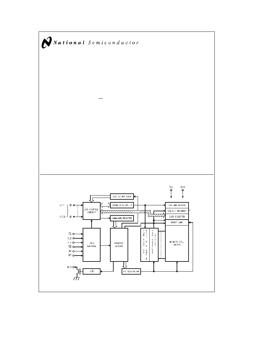
General Description
The NM29N16 is a 16 Mbit (2 Mbyte) NAND FLASH The
device is organized as an array of 512 blocks each consist-
ing of 16 pages Each page contains 264 bytes All com-
mands and data are sent through eight I O pins To read
data a page is first transferred out of the array to an on-chip
buffer Sending successive read pulses (RE low) reads out
successive bytes of data The erase operation is implement-
ed in either a single block (4 kbytes) or on multiple blocks at
the same time Programming the device requires sending
address and data information to the on-board buffer and
then issuing the program command Typical program time
for 264 bytes is 400 ms All erase and program operations
are internally timed
The NM29N16 incorporates a number of features that make
it ideal for portable applications requiring high density stor-
age These features include single 5V operation high read
write endurance (250k cycle) and low current operation
(15 mA during reads) The device comes in a TSOP Type II
package which meets the requirements of PCMCIA cards
The NM29N16 is suited for numerous applications such as
Solid State Drives (SSD) Audio Recording and Image Stor-
age for digital cameras
Features
Y
Single 5V
g
10% power supply
Y
Write Erase endurance of 250 000 cycles
target of
1 000 000 cycles
Y
Fast Erase Program Times
Average Program Time of 400 ms 264 bytes
Typical Block Erase Time of 6 ms
Y
Organized as 512 blocks each consisting of 16 pages
of 264 bytes
Read Program in pages of 264 bytes
Erase in Blocks of 4 kbytes
Y
High Performance Read Access times
Initial 25 ms page transfer
Sequential 80 ns access
Y
Low Operating Current (typical)
Typical Read current of 15 mA
Typical Program current of 40 mA
Typical Erase current of 20 mA
Standby current less than 100 mA (CMOS)
Y
Command Register for Mode Control
Read
Reset
Auto Page Program
Suspend Resume
Auto Block Erase
Status Read
Y
400 mil TSOP Type II Package
Y
JEDEC standard pinout
Block Diagram
TL D 11915 ≠ 1
C1996 National Semiconductor Corporation
RRD-B30M56 Printed in U S A

Pin Connection
(Top View)
NM29N16S
TL D 11915 ≠ 2
NM29N16R
TL D 11915 ≠ 3
Pin Assignment
I O
I ≠ 8
I O Port
CE
Chip Enable
WE
Write Enable
RE
Read Enable
CLE
Command Latch Enable
ALE
Address Latch Enable
WP
Write Protect
R B
Ready Busy
V
CC
V
SS
Power Supply Ground
TL D 11915 ≠ 85
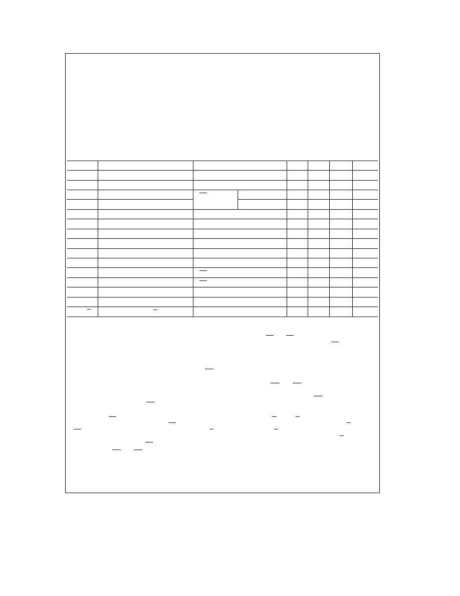
Number of Valid Blocks
(1)
Symbol
Parameter
NM29N16
Units
Min
Typ
Max
N
VB
Valid Block Number
502
508
512
Blocks
Note 1
The NM29N16S R may include unusable blocks Refer to notification (17) toward the end of this document
Capacitance
(T
A
e a
25 C f
e
1 MHz)
Symbol
Parameter
Condition
Min
Type
Max
Units
C
IN
Input
V
IN
e
0V
5
10
pF
C
OUT
Output
V
OUT
e
0V
5
10
pF
This parameter is periodically sampled and is not 100% tested
http
www national com
2
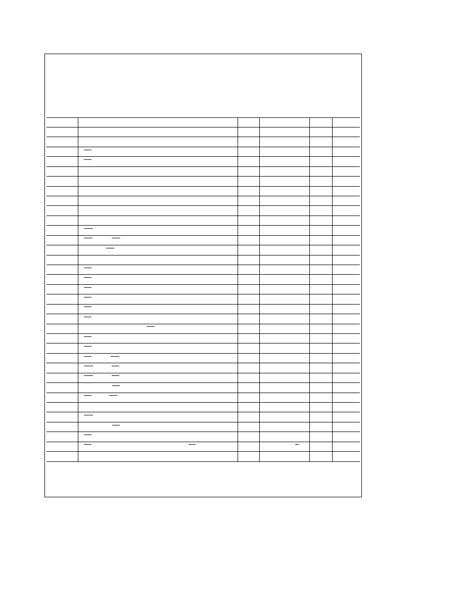
Absolute Maximum Ratings
If Military Aerospace specified devices are required
please contact the National Semiconductor Sales
Office Distributors for availability and specifications
Power Supply (V
CC
)
b
0 6V to 7 0V
Input Voltage (V
IN
)
b
0 6V to 7 0V
Input Output Voltage (V
I O
)
b
0 6V to V
CC
g
0 5V (
s
7V)
Power Dissipation (P
D
)
0 5W
Soldering Temperature (T
solder
) (10 seconds)
260 C
Storage Temperature (T
stg
)
b
55 C to 150 C
Operating Temperature (T
opr
)
0 C to 70 C
Recommended Operating
Conditions
Min
Typ
Max
Units
Power Supply (V
CC
)
4 5
5 0
5 5
V
High Level Input Voltage (V
IH
)
2 4
V
CC
a
0 5
V
Low Level Input Voltage (V
IL
)
b
0 3
0 8
V
b
2V (Pulse Width
k
20 ns)
DC Operating Characteristics
(T
A
e
0 C to 70 C V
CC
e
5V
g
10%)
Symbol
Parameter
Conditions
Min
Typ
Max
Units
I
LI
Input Leakage Current
V
IN
e
0V to V
CC
g
10
m
A
I
LO
Output Leakage Current
V
OUT
e
0 4V to V
CC
g
10
m
A
I
CC01
Operating Current (Serial Read)
CE
e
V
IL
t
CYCLE
e
80 ns
15
30
mA
I
CC02
Operating Current (Serial Read)
I
OUT
e
0 mA
t
CYCLE
e
1 ms
5
mA
I
CC03
Operating Current (Command Input)
t
CYCLE
e
80 ns
15
30
mA
I
CC04
Operating Current (Data Input)
t
CYCLE
e
80 ns
50
70
mA
I
CC05
Operating Current (Address Input)
t
CYCLE
e
80 ns
15
30
mA
I
CC06
Operating Current (Register Read)
t
CYCLE
e
80 ns
15
30
mA
I
CC07
Programming Current
40
60
mA
I
CC08
Erasing Current
20
40
mA
I
CCS1
Standby Current
CE
e
V
IH
1
mA
I
CCS2
Standby Current
CE
e
V
CC
b
0 2V
100
m
A
V
OH
High Level Output Voltage
I
OH
e b
400 mA
2 4
V
V
OL
Low Level Output Voltage
I
OL
e
2 1 mA
0 4
V
I
OL
(R B)
Output Current of (R B) Pin
V
OL
e
0 4V
10
mA
Pin Functions
The NM29N16 is a sequential access memory which utilizes
time sharing input of address and data information
Command Latch Enable CLE
The CLE input signal is
used to control the input of commands into the internal
command register The command is latched into the com-
mand register from the I O port at the rising edge of the WE
signal while CLE is high
Address Latch Enable ALE
The ALE signal is used to
control the input of either address information or input data
into the internal address data register Address information
is latched at the rising edge of WE if ALE is high Input data
is latched if ALE is low
Chip Enable CE
The device goes into a low power stand-
by mode during a read operation when CE goes high The
CE signal is ignored when the device is in a busy state (R B
e
L) such as during a program or erase operation and will
not go into standby mode if a CE high signal is input
Write Enable
WE
The WE signal is used to strobe data
into the I O port
Read Enable RE
The RE signal strobes data output Data
is available t
REA
after the falling edge of RE The internal
column address counter is also incremented (Address
a
1)
with this falling edge
I O Port I O 1 ≠ 8
The I O 1 ≠ 8 pins are used as the port for
transferring address command and input output data infor-
mation to or from the device
Write Protect
WP
The WP signal is used to protect the
device from inadvertent programming or erasing The inter-
nal voltage regulator is reset when WP is low This signal is
usually used for protecting the data during the power on off
sequence when the input signals are invalid
Ready Busy R B
The R B output signal is used to indi-
cate the operating condition of the device The R B signal is
in a busy state (R B
e
L) during the program erase or read
operations and will return to a ready state (R B
e
H) after
completion The output buffer of this signal is an open drain
http
www national com
3
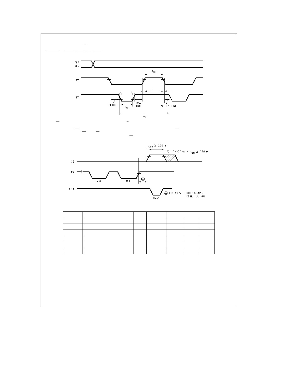
AC Test Conditions
Input Level
2 4V 0 4V
Input Comparison Level
2 2V 0 8V
Output Data Comparison Level
2 0V 0 8V
Output Load
1TTL
C
L
(100 pF)
AC Electrical Characteristics
(T
A
e
0 C to 70 C V
CC
e
5V
g
10%)
Symbol
Parameter
Min
Max
Unit
Notes
t
CLS
CLE Setup Time
20
ns
t
CLH
CLE Hold Time
40
ns
t
CS
CE Setup Time
20
ns
t
CH
CE Hold Time
40
ns
t
WP
Write Pulse Width
40
ns
t
ALS
ALE Setup Time
20
ns
t
ALH
ALE Hold Time
40
ns
t
DS
Data Setup Time
30
ns
t
DH
Data Hold Time
20
ns
t
WC
Write Cycle Time
80
ns
(1)
t
WH
WE High Hold Time
20
ns
t
WW
WP High to WE Falling Edge
100
ns
t
RR
Ready to RE Falling Edge
20
ns
t
RC
Read Cycle Time
80
ns
t
REA
RE Access Time (Serial Data Access)
45
ns
t
CEH
CE High Time at the Last Address in Serial Read Cycle
250
ns
(3)
t
REAID
RE Access Time (ID Read)
90
ns
t
RHZ
RE High to Output High Impedance
5
20
ns
t
CHZ
CE High to Output High Impedance
30
ns
t
REH
RE High Hold Time
20
ns
t
IR
Output High Impedance to RE Rising Edge
0
ns
t
RSTO
RE Access Time (Status Read)
45
ns
t
CSTO
CE Access Time (Status Read)
55
ns
t
RHW
RE High to WE Low
0
ns
t
WHC
WE High to CE Low
50
ns
t
WHR
WE High to RE Low
50
ns
t
AR1
ALE Low to RE Low (Address Register Read ID Read)
200
ns
t
CR
CE Low to RE Low (Address Register Read ID Read)
200
ns
t
R
Memory Cell Array to Starting Address
25
m
s
t
WB
WE High to Busy
200
ns
t
AR2
ALE Low to RE low (Read Cycle)
150
ns
t
RB
RE Last Clock Rising Edge to Busy (At Sequential Read)
200
ns
t
CRY
CE High to Ready (in case of interception by CE at Read Mode)
100
a
tr(R B)
ns
(2)
t
RST
Device Reset Time (Read Program Erase Suspend)
10 20 1500 10
m
s
http
www national com
4
AC Electrical Characteristics
(T
A
e
0 C to
a
70 C V
CC
e
5V
g
10%) (Continued)
Note 1
In case that CLE ALE CE are input with clock t
WC
exceeds 80 ns Transition time t
T
s
5 ns
set-up time
20 ns
a
hold time
40 ns
a
t
WP
40 ns
a
t
XX
a
4t
T
20 ns
TL D 11915 ≠ 5
Note 2
CE high to Ready time depends on Pull up resister tied to R B pin (Refer to notification (10) toward the end of this document )
Note 3
In the case that CE turns to a high level after accessing the last address (263) in read mode (1) or (2) CE high time must keep equal to or greater than
300 ns when the delay time of CE against RE is 0 to 200 ns as shown below
In the second case the device will not turn to a ``Busy'' state when the CE delay time is less than 30 ns
TL D 11915 ≠ 6
Programming and Erasing Characteristic
(T
A
e
0 C to
a
70 C V
CC
e
5V
g
10%)
Symbol
Parameter
Min
Typ
Max
Unit
Notes
t
PROG
Average Programming Time
300 ≠ 1000
5000
m
s
N
Divided Number on Same Page
10
Cycles
(1)
t
BERASE
Block Erasing Time
6
6
100
ms
t
MBERASE
Multi-Block Erasing Time
6 ≠ 12
6 ≠ 12
130
ms
(2)
t
SR
Suspend Input to Ready
1 5
ms
N
W E
Number Write Erase Cycles
2 5 x 10
5
Cycles
Note 1
Refer to the notification (16) toward the end of this document
Note 2
t
MBERASE
depends on the number of blocks to be erased (min 6 ms
a
15 ms x Erase block number)
http
www national com
5