TL D 10045
NM93C06LC46LC56LC66L
256-1024-2048-4096-Bit
Serial
EEPROM
with
Extended
Voltage
(27V
to
55V)
(MICROWIRE
Bus
Interface)
November 1996
NM93C06L C46L C56L C66L
256- 1024- 2048- 4096-Bit Serial EEPROM
with Extended Voltage (2 7V to 5 5V)
(MICROWIRE
TM
Bus Interface)
General Description
The
NM93C06L C46L C56L C66L
devices
are
256 1024 2048 4096 bits
respectively
of non-volatile
electrically erasable memory divided into 16 64 128 256 x
16-bit registers (addresses) The NM93CxxL Family func-
tions in an extended voltage operating range requires only
a single power supply and is fabricated using National Semi-
conductor's floating gate CMOS technology for high reliabili-
ty high endurance and low power consumption These de-
vices are available in both SO and TSSOP packages for
small space considerations
The EEPROM Interfacing is MICROWIRE compatible for
simple interface to standard microcontrollers and micro-
processors There are 7 instructions that control these de-
vices Read Erase Write Enable Erase Erase All Write
Write All and Erase Write Disable The ready busy status
is available on the DO pin during programming
Features
Y
2 7V to 5 5V operation in all modes
Y
Typical active current of 100 mA Typical standby
current of 1 mA
Y
No erase required before write
Y
Reliable CMOS floating gate technology
Y
MICROWIRE compatible serial I O
Y
Self-timed programming cycle
Y
Device status during programming mode
Y
40 years data retention
Y
Endurance 10
6
data changes
Y
Packages available
8-pin SO
8-pin DIP
and 8-pin
TSSOP
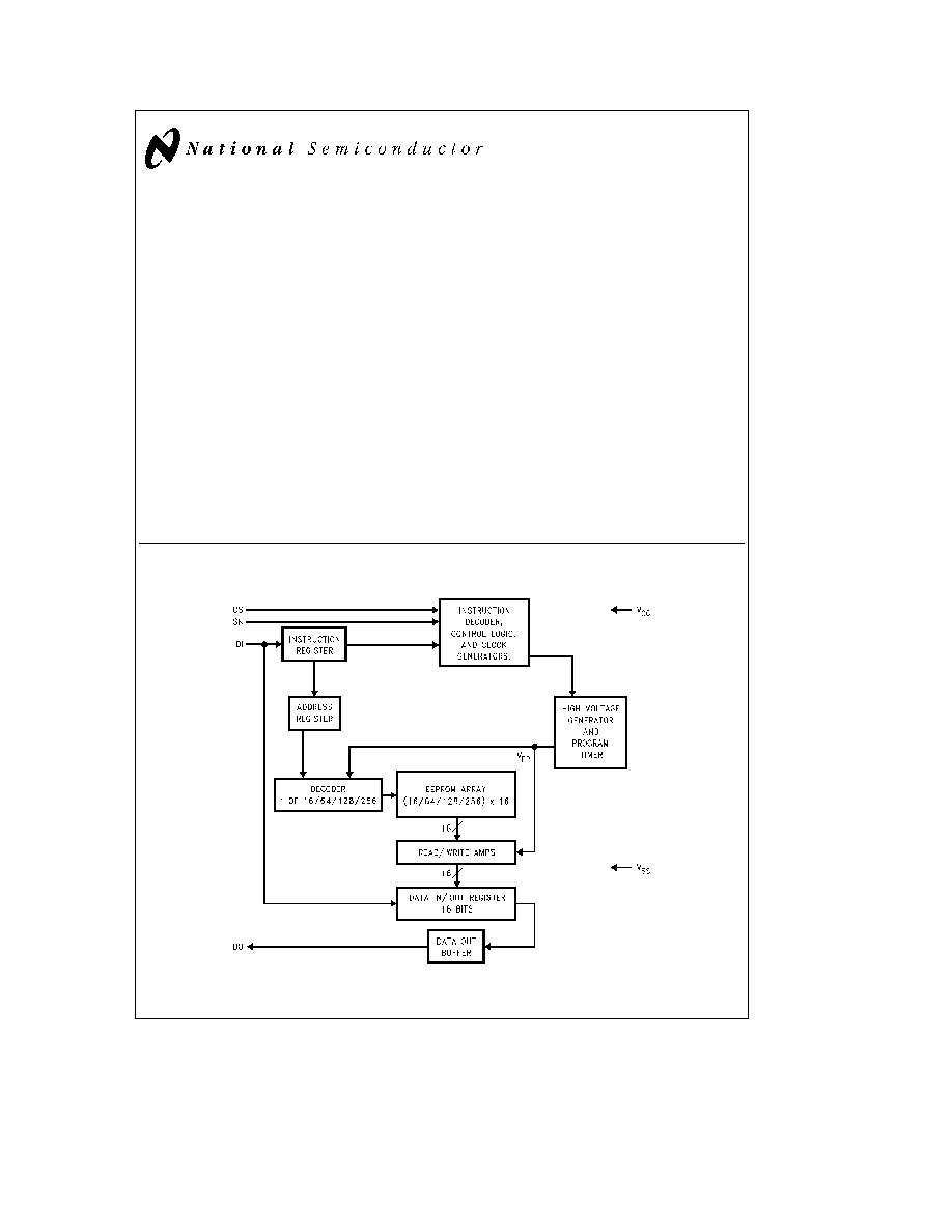
Block Diagram
TL D 10045 � 1
TRI-STATE
is a registered trademark of National Semiconductor Corporation
MICROWIRE
TM
is a trademark of National Semiconductor Corporation
C1996 National Semiconductor Corporation
RRD-B30M126 Printed in U S A
http
www national com
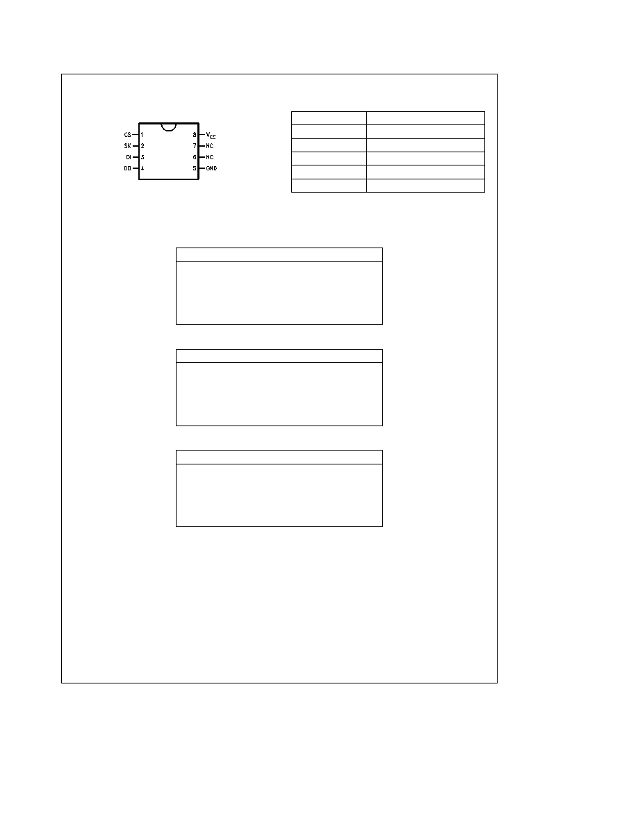
Connection Diagrams
Dual-In-Line Package (N)
8-Pin SO (M8) and 8-Pin TSSOP (MT8)
TL D 10045 � 2
Top View
NS Package Number N08E M08A or MTC08
Pin Names
CS
Chip Select
SK
Serial Data Clock
DI
Serial Data Input
DO
Serial Data Output
GND
Ground
V
CC
Power Supply
Ordering Information
Commercial Temp Range (0 C to
a
70 C)
Order Number
NM93C06LN NM93C46LN
NM93C56LN NM93C66LN
NM93C06LM8 NM93C46LM8
NM93C56LM8 NM93C66LM8
NM93C06LMT8 NM93C46LMT8
NM93C56LMT8 NM93C66LMT8
Extended Temp Range (
b
40 C to
a
85 C)
Order Number
NM93C06LEN NM93C46LEN
NM93C56LEN NM93C66LEN
NM93C06LEM8 NM93C46LEM8
NM93C56LEM8 NM93C66LEM8
NM93C06LEMT8 NM93C46LEMT8
NM93C56LEMT8 NM93C66LEMT8
Automotive Temp Range (
b
40 C to
a
125 C)
Order Number
NM93C06LVN NM93C46LVN
NM93C56LVN NM93C66TLVN
NM93C06LVM8 NM93C46LVM8
NM93C56LVM8 NM93C66LVM8
NM93C06LVMT8 NM93C46LVMT8
NM93C56LVMT8 NM93C66LVMT8
http
www national com
2
Absolute Maximum Ratings
(Note 1)
If Military Aerospace specified devices are required
please contact the National Semiconductor Sales
Office Distributors for availability and specifications
Ambient Storage Temperature
b
65 C to
a
150 C
All Input or Output Voltages
a
6 5V to
b
0 3V
with Respect to Ground
Lead Temp (Soldering 10 sec )
a
300 C
ESD Rating
2000V
Operating Conditions
Ambient Operating Temperature
NM93C06L � NM93C66L
0 C to
a
70 C
NM93C06LE � NM93C66LE
b
40 C to
a
85 C
NM93C06LV � NM93C66LV
b
40 C to
a
125 C
Power Supply (V
CC
) Range
2 7V to 5 5V
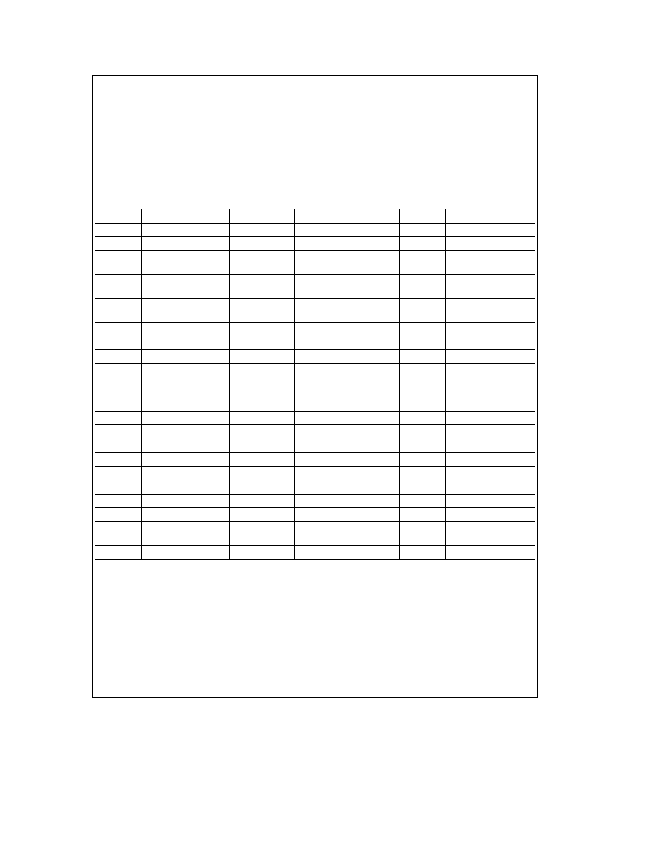
DC and AC Electrical Characteristics 2 7 V
k
V
CC
k
4 5V
Symbol
Parameter
Part Number
Conditions
Min
Max
Units
I
CCA
Operating Current
CS
e
V
IH
SK
e
250 kHz
1
mA
I
CCS
Standby Current
CS
e
V
IL
10
m
A
I
IL
Input Leakage
V
IN
e
0V to V
CC
g
1
m
A
I
OL
Output Leakage
V
IL
Input Low Voltage
b
0 1
0 15 V
CC
V
V
IH
Input High Voltage
0 8 V
CC
V
CC
a
1
V
OL
Output Low Voltage
I
OL
e
10 mA
0 1 V
CC
V
V
OH
Output High Voltage
I
OH
e b
10 mA
0 9 V
CC
f
SK
SK Clock Frequency
0
250
kHz
t
SKH
SK High Time
1
m
s
t
SKL
SK Low Time
1
m
s
t
SKS
SK Setup Time
SK Must Be at V
IL
for
0 2
m
s
t
SKS
before CS goes high
t
CS
Minimum CS
(Note 2)
1
m
s
Low Time
t
CSS
CS Setup Time
0 2
m
s
t
DH
DO Hold Time
70
ns
t
DIS
DI Setup Time
0 4
m
s
t
CSH
CS Hold Time
0
m
s
t
DIH
DI Hold Time
0 4
m
s
t
PD1
Output Delay to ``1''
2
m
s
t
PD0
Output Delay to ``0''
2
m
s
t
SV
CS to Status Valid
1
m
s
t
DF
CS to DO in
CS
e
V
IL
0 4
m
s
TRI-STATE
t
WP
Write Cycle Time
15
ms
http
www national com
3
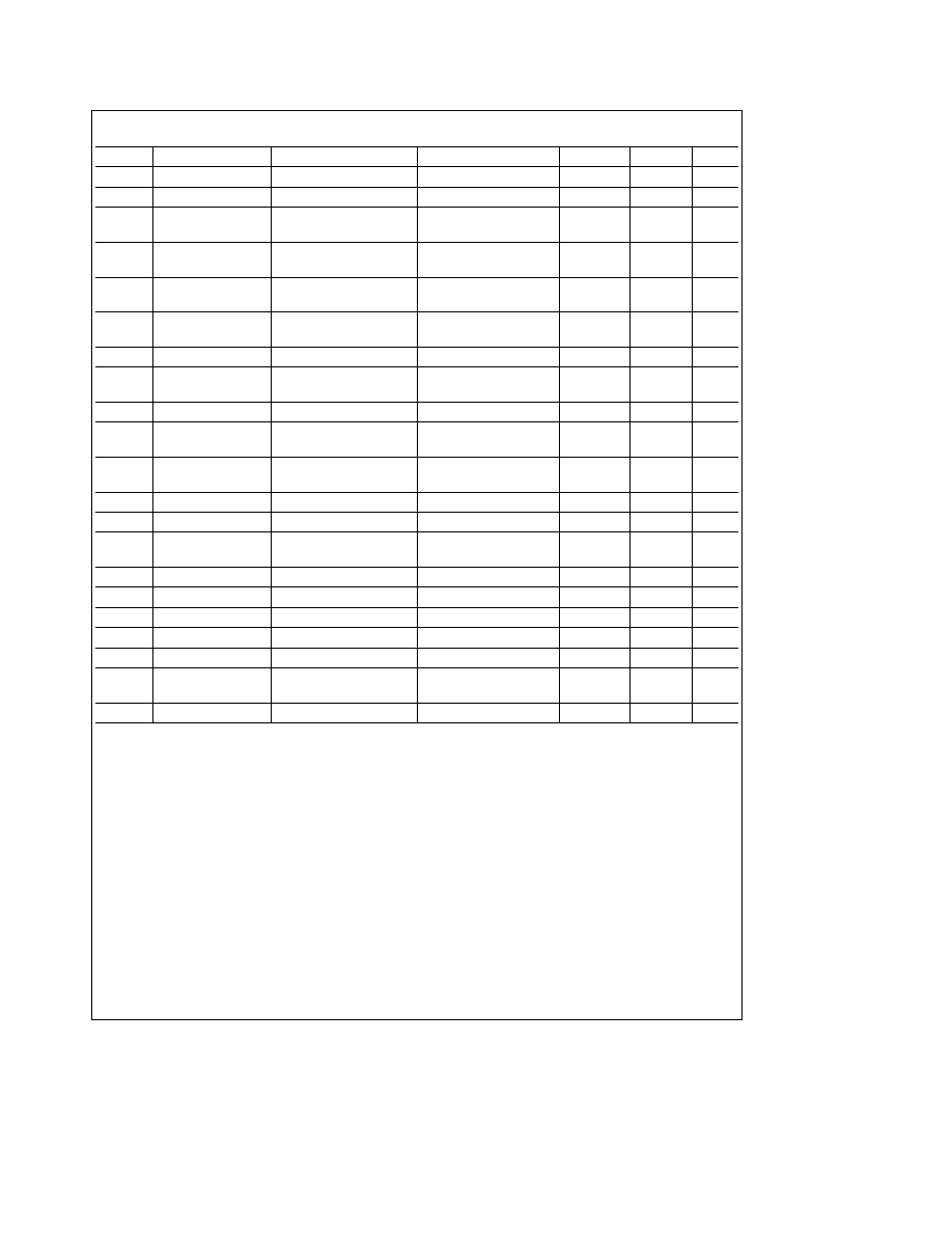
DC and AC Electrical Characteristics 4 5V
k
V
CC
k
5 5V
Symbol
Parameter
Part Number
Conditions
Min
Max
Units
I
CCA
Operating Current
CS
e
V
IH
SK
e
1 MHz
1
mA
I
CCS
Standby Current
CS
e
V
IL
50
m
A
I
IL
Input Leakage
V
IN
e
0V to V
CC
g
1
m
A
I
OL
Output Leakage
(Note 4)
V
IL
Input Low Voltage
b
0 1
0 8
V
V
IH
Input High Voltage
2
V
CC
a
1
V
OL1
Output Low Voltage
I
OL
e
2 1 mA
0 4
V
V
OH1
Output High Voltage
I
OH
e b
400 mA
2 4
V
OL2
Output Low Voltage
I
OL
e
10 mA
0 2
V
V
OH2
Output High Voltage
I
OL
e b
10mA
V
CC
b
0 2
f
SK
SK Clock Frequency
(Note 5)
0
1
MHz
t
SKH
SK High Time
NM93C06L-NM93C66L
250
ns
NM93C06LE-NM93C66LE
300
t
SKL
SK Low Time
250
ns
t
SKS
SK Setup TIme
SK Must Be at V
IL
for
50
ns
t
SKS
before CS goes high
t
CS
Minimum CS
(Note 2)
250
ns
Low Time
t
CSS
CS Setup Time
50
ns
t
DH
DO Hold Time
70
ns
t
DIS
DI Setup Time
NM93C06L-NM93C66L
100
ns
NM93C06LE-NM93C66LE
200
t
CSH
CS Hold Time
0
ns
t
DIH
DI Hold Time
20
ns
t
PD1
Output Delay to ``1''
500
ns
t
PD0
Output Delay to ``0''
500
ns
t
SV
CS to Status Valid
500
ns
t
DF
CS to DO in
100
ns
TRI-STATE
CS
e
V
IL
t
WP
Write Cycle Time
10
ms
http
www national com
4
Capacitance
(Note 3)
T
A
e
25 C f
e
1 MHz
Symbol
Test
Typ
Max
Units
C
OUT
Output Capacitance
5
pF
C
IN
Input Capacitance
5
pF
Note 1
Stress above those listed under ``Absolute Maximum Ratings'' may cause permanent damage to the device This is a stress rating only and operation of the
device at these or any other conditions above those indicated in the operational sections of the specification is not implied Exposure to absolute maximum rating
conditions for extended periods may affect device reliability
Note 2
CS (Chip Select) must be brought low (to V
IL
) for an interval of t
CS
in order to reset all internal device registers (device reset) prior to beginning another
opcode cycle (this is shown in the opcode diagrams in the following pages)
Note 3
This parameter is periodically sampled and not 100% tested
Note 4
Typical leakage values are in the 20 nA range
Note 5
The shortest allowable SK clock period
e
1 f
SK
(as shown under the f
SK
parameter) Maximum SK clock speed (minimum SK period) is determined by the
interaction of several AC parameters stated in the datasheet Within this SK period both t
SKH
and t
SKL
limits must be observed Therefore it is not allowable to set
1 t
SK
e
t
SKH (minimum)
a
t
SKL (minimum)
for shorter SK cycle time operation
AC Test Conditions
V
CC
Range
V
IL
V
IH
V
IL
V
IH
V
OL
V
OH
I
OL
I
OH
Input Levels
Timing Levels
Timing Levels
2 7V
s
V
CC
k
4 5V
0 3V 1 8V
1 0V
0 8V 1 5V
g
10 mA
(Extended Voltage Levels)
4 5V
s
V
CC
s
5 5V
0 4V 2 4V
1 0V 2 0V
0 4V 2 4V
b
2 1 mA 0 4 mA
(TTL Levels)
Output Load 1 TTL Gate (C
L
e
100 pF)
Functional Description
The NM93C06L C46L C56L C66L device have 7 instruc-
tions as described below Note that the MSB of any instruc-
tion is a ``1'' and is viewed as a start bit in the interface
sequence For the C06 and C46 the next 8 bits carry the op
code and the 6-bit address for register selection For the
C56 and C66 the next 10-bits carry the op code and the 8-
bit address for register selection
Read (READ)
The READ instruction outputs serial data on the DO pin
After a READ instruction is received the instruction and ad-
dress are decoded followed by data transfer from the se-
lected memory register into a 16-bit serial-out shift register
A dummy bit (logical 0) precedes the 16-bit data output
string Output data changes are initiated by a low to high
transition of the SK clock
Erase Write Enable (WEN)
When V
CC
is applied to the part it powers up in the Erase
Write Disable (WDS) state Therefore all programming
modes must be preceded by an Erase Write Enable WEN
instruction Once an Erase Write Enable instruction is exe-
cuted programming remains enabled until an Erase Write
Disable (WDS) instruction is executed or V
CC
is completely
removed from the part
Erase (ERASE)
The ERASE instruction will program all bits in the selected
register to the logical ``1'' state CS is brought low following
the loading of the last address bit This falling edge of the
CS pin initiates the self-timed programming cycle
The DO pin indicates the READY BUSY status of the chip if
CS is brought high after the t
CS
interval DO
e
logical ``0''
indicates that programming is still in progress DO
e
logical
``1'' indicates that the register at the address specified in
the instruction has been erased and the part is ready for
another instruction
http
www national com
5

Functional Description
(Continued)
Write (WRITE)
The WRITE instruction is followed by 16 bits of data to be
written into the specificed address After the last bit of data
is put on the data-in (DI) pin CS must be brought low before
the next rising edge of the SK clock This falling edge of CS
initiates the self-timed programming cycle The DO pin indi-
cates the READY BUSY status of the chip if CS is brought
high after the t
CS
interval DO
e
logical 0 indicates that
programming is still in progress DO
e
logical 1 indicates
that the register at the address specified in the instruction
has been written with the data pattern specified in the in-
struction and the part is ready for another instruction
Erase All (ERAL)
The ERAL instruction will simultaneously program all regis-
ters in the memory array and set each bit to the logical ``1''
state The Erase All cycle is identical to the ERASE cycle
except for the different op-code As in the ERASE mode
the DO pin indicates the READY BUSY status of the chip if
CS is brought high after the t
CS
interval
Write All (WRALL)
The WRALL instruction will simultaneously program all reg-
isters with the data pattern specified in the instruction As in
the WRITE mode the DO pin indicates the READY BUSY
status of the chip if CS is brought high after the t
CS
interval
Write Disable (WDS)
To protect against accidental data distrub the WDS instruc-
tion disables all programming modes and should follow all
programming operations Execution of a READ instruction is
independent of both the WEN and WDS instructions
Note
NSC CMOS EEPROMs do not require an ``ERASE'' or ``ERASE ALL'' operation prior to the ``WRITE'' and ``WRITE ALL'' instructions The ``ERASE'' and
``ERASE ALL'' instructions are included to maintain compatibility with earlier technology EEPROMs
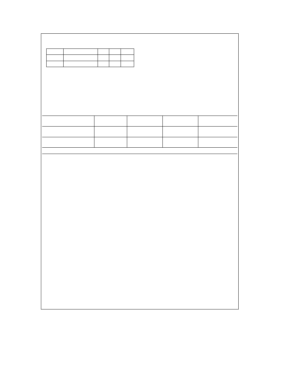
Instruction Set for the NM93C06L and NM93C46L
Instruction
SB
Op Code
Address
Data
Comments
READ
1
10
A5 � A0
Reads data stored in memory at specified address
WEN
1
00
11XXXX
Enable all programming modes
ERASE
1
11
A5 � A0
Erase selected register
WRITE
1
01
A5 � A0
D15 � D0
Writes selected register
ERAL
1
00
10XXXX
Erases all registers
WRALL
1
00
01XXXX
D15 � D0
Writes all registers
WDS
1
00
00XXXX
Disables all programming modes
Note
Address bits A5 and A4 become ``Don't Care'' for the NM93C06L
Instruction Set for the NM93C56L and NM93C66L
Instruction
SB
Op Code
Address
Data
Comments
READ
1
10
A7 � A0
Reads data stored in memory at specified address
WEN
1
00
11XXXXXX
Enable all programming modes
ERASE
1
11
A7 � A0
Erase selected register
WRITE
1
01
A7 � A0
D15 � D0
Writes selected register
ERAL
1
00
10XXXXXX
Erases all registers
WRALL
1
00
01XXXXXX
D15 � D0
Writes all registers
WDS
1
00
00XXXXXX
Disables all programming modes
Note
Address bit A7 is ``Don't Care'' for the NM93C56L
http
www national com
6
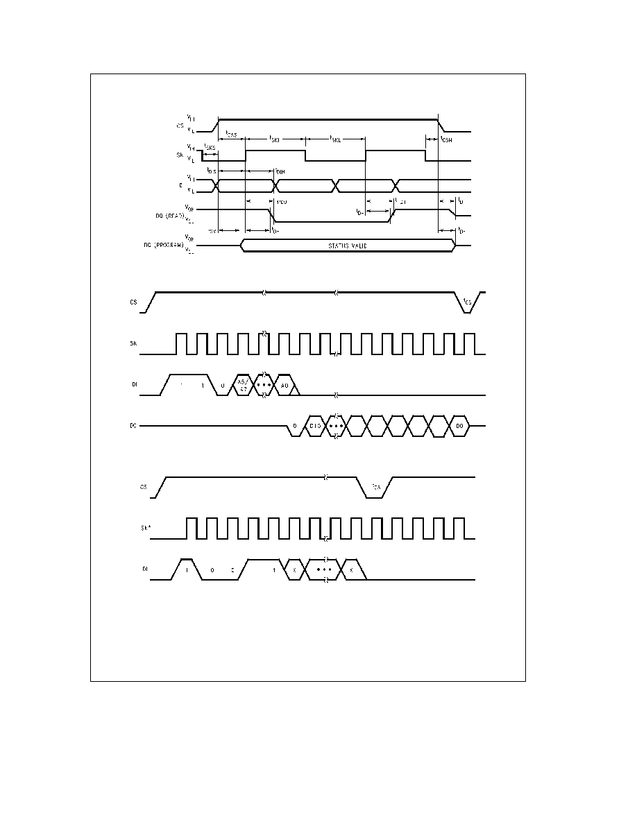
Timing Diagrams
Synchronous Data Timing
TL D 10045 � 13
READ
TL D 10045 � 5
WEN
TL D 10045 � 6
http
www national com
7
Timing Diagrams
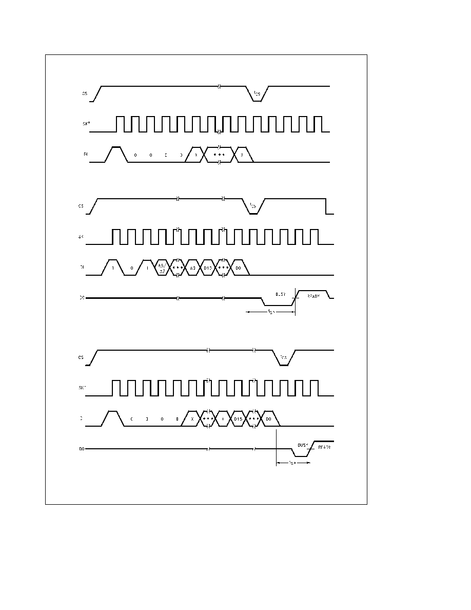
(Continued)
WDS
TL D 10045 � 7
WRITE
TL D 10045 � 8
WRALL
TL D 10045 � 9
http
www national com
8
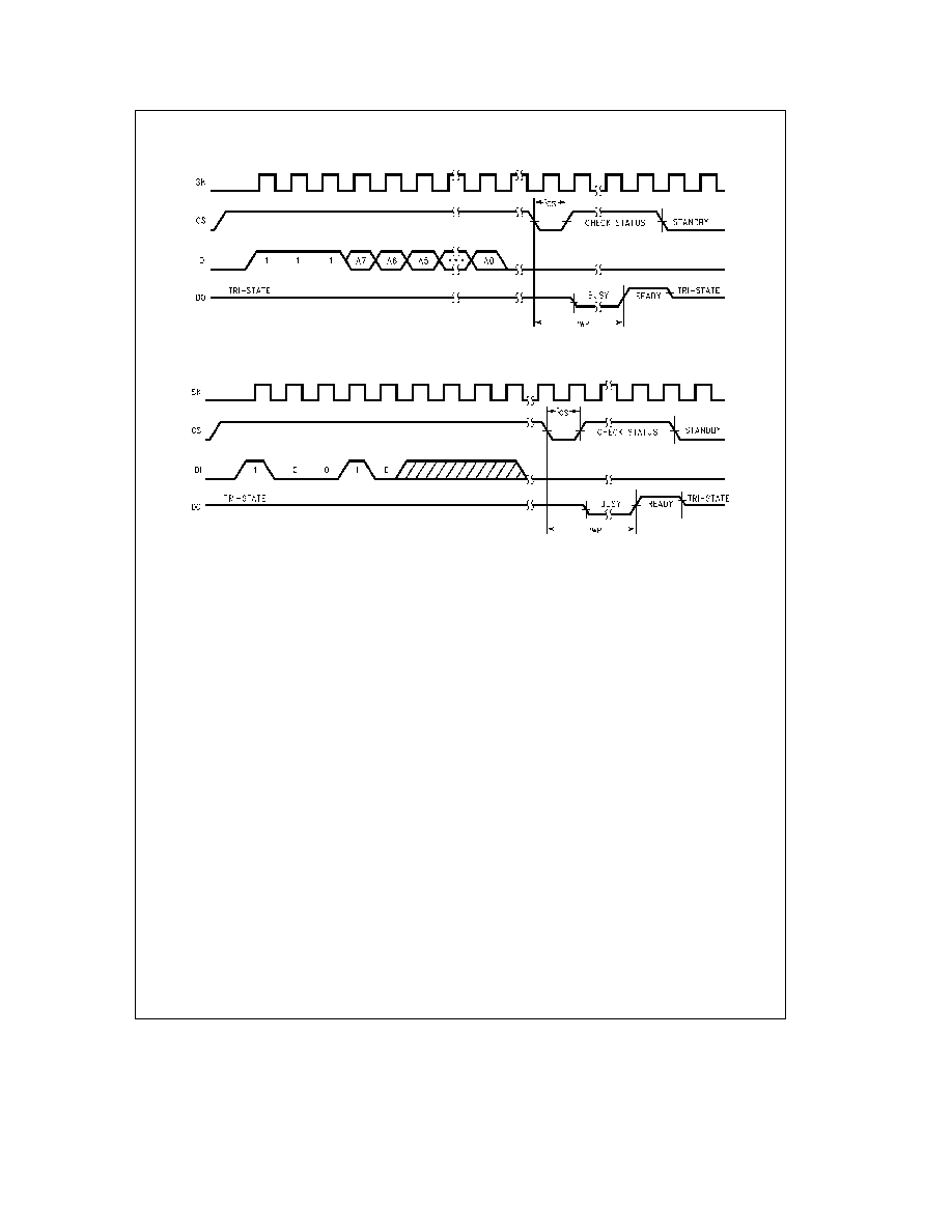
Timing Diagrams
(Continued)
ERASE
TL D 10045 � 10
ERAL
TL D 10045 � 11
http
www national com
9
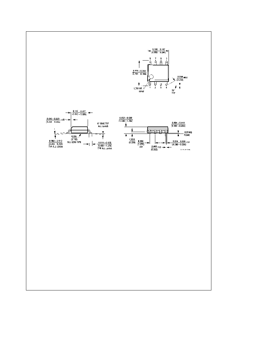
Physical Dimensions
inches (millimeters) unless otherwise noted
Molded Small Out-Line Package (M8)
NS Package Number M08A
http
www national com
10
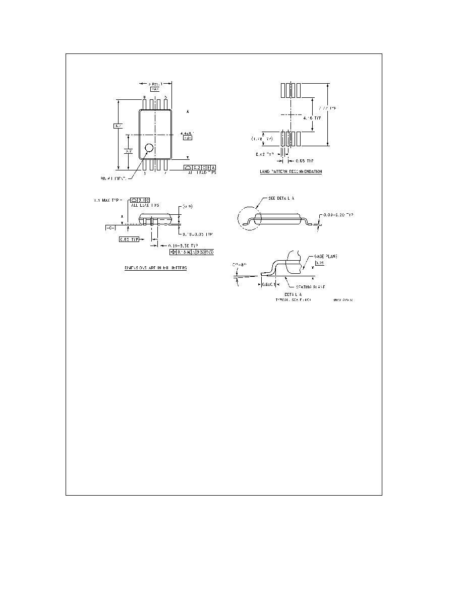
Physical Dimensions
inches (millimeters) unless otherwise noted (Continued)
Notes Unless otherwise specified
1 Reference JEDEC Registration M0-153 Variation AA Dated 7 93
8-Pin Molded TSSOP JEDEC (MT8)
NS Package Number MTC08
http
www national com
11
NM93C06LC46LC56LC66L
256-1024-2048-4096-Bit
Serial
EEPROM
with
Extended
Voltage
(27V
to
55V)
(MICROWIRE
Bus
Interface)
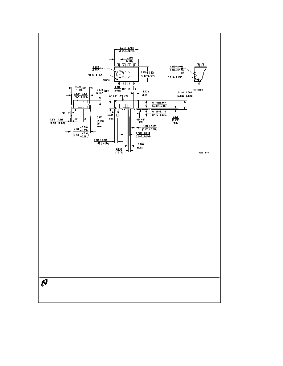
Physical Dimensions
inches (millimeters) unless otherwise noted (Continued)
Molded Dual-In-Line Package (N)
NS Package Number N08E
LIFE SUPPORT POLICY
NATIONAL'S PRODUCTS ARE NOT AUTHORIZED FOR USE AS CRITICAL COMPONENTS IN LIFE SUPPORT
DEVICES OR SYSTEMS WITHOUT THE EXPRESS WRITTEN APPROVAL OF THE PRESIDENT OF NATIONAL
SEMICONDUCTOR CORPORATION As used herein
1 Life support devices or systems are devices or
2 A critical component is any component of a life
systems which (a) are intended for surgical implant
support device or system whose failure to perform can
into the body or (b) support or sustain life and whose
be reasonably expected to cause the failure of the life
failure to perform when properly used in accordance
support device or system or to affect its safety or
with instructions for use provided in the labeling can
effectiveness
be reasonably expected to result in a significant injury
to the user
National Semiconductor
National Semiconductor
National Semiconductor
National Semiconductor
Corporation
Europe
Southeast Asia
Japan Ltd
Fax a49 (0) 180-530 85 86
Fax (852) 2376 3901
Tel 81-3-5620-7561
Americas
Email europe support nsc com
Email sea support nsc com
Fax 81-3-5620-6179
Tel 1(800) 272-9959
Deutsch Tel a49 (0) 180-530 85 85
Fax 1(800) 737-7018
English
Tel a49 (0) 180-532 78 32
Email support nsc com
Fran ais Tel a49 (0) 180-532 93 58
Italiano
Tel a49 (0) 180-534 16 80
http
www national com
National does not assume any responsibility for use of any circuitry described no circuit patent licenses are implied and National reserves the right at any time without notice to change said circuitry and specifications